High-Resolution, Analytical STEM/SEM Providing Simultaneous Chemical and Bonding Analysis, Atomic Resolution, and Surface Imaging at 30kV and below
Investigating samples with the full capabilities of STEM at 30 keV and below is an extremely interesting and rapidly growing area of research: providing both Materials and Life Sciences with full SEM and STEM, inclusive EDX, and EELS capabilities, at low voltages. Less beam damage and higher contrast are the key arguments for the Low-Voltage STEM (LV-STEM), a capability that has been out of reach for researchers globally. With the LV-STEM, its low beam energy, increased contrast, and narrow energy spread, investigations of biological material in an unstained condition are becoming a reality for the first time.
Since the STEM unit has no imaging lens after the sample, electrons that were inelastically scattered by the sample do not really worsen image quality (they do for TEM). The significance of the lack of chromatic aberrations after the sample increases with decreasing electron energy; samples that typically would require a 100-keV TEM, at the very least, can be investigated with low-keV STEM. Multi-scattering processes and absorption of course still appear—ultimately limiting the acceptable thickness of the specimen. However, the use of high-end specimen preparation techniques, or working with thin samples as is typical in nano-research fields, allows 30-keV STEMs to cover much of the areas of conventional higher-keV TEMs, while at the same time, providing surface information through standard SEM methods, including SE, BSE, and high-angle BSE.
The well-established cold FEG of Hitachi’s high-end SEMs is a tremendous benefit for EELS capabilities as well as the point resolution of STEM. Despite the unusually low voltage for EELS and the increased impact of environmental conditions on low-voltage electrons, we are able to demonstrate better than 400-meV FWHM (full width half maximum, see Figure 1, left) for the ZLP (zero loss peak) of EELS, allowing clear and crisp EELS data for fine structure investigations. For example, eliciting the tiny changes in the π bonding for the Graphene as layer after layer is added demonstrates the sensitivity of the LV-STEM (see Figure 1, right). The LV-STEM also has a 2nd dedicated EELS detector with 3 elements, allowing the rapid (10,000 fps) acquisition of energy-filtered BF STEM images, Plasmon images, or the rapid collection of elemental maps. Switching between both detectors is easy and relies on Hitachi’s own unique design.
The LV-STEM feature (Figure 2) complements SE imaging and makes no compromise. Typical images taken at 30 keV without a Cs corrector or Cc corrector approach 0.2-nm resolution establishing the LV-STEM as the true performance leader for ≤ 30 keV microscopy. The importance of simultaneously acquiring STEM and SE data is demonstrated in Figure 3.
As this microscope can handle samples up to 5.0 mm × 9.5 mm × 3.5 mm, the optional windowless EDX detector supports the analysis of both thin and bulk areas. At an incredible collection angle of 0.7 sr, acquisition times for EDX maps are short (see details in Figure 4), making the LV-STEM a truly ground-breaking microscope for both Materials and Life Sciences applications.
References
- 1)
- R.F. Egerton, “Electron Energy-Loss Spectroscopy in Electron Microscope”, Springer, New York
- 2)
- K. Suenaga et al., Nature, Vol.468 (2010), 1088-1090
- 3)
- G. Algara-Siller, O. Lehtinen, A. Turchanin and U. Kaiser, (2014). Appl. Phys. Lett., 104, 153115.
- 4)
- The authors wish to thank Dr. Tsuyohiko Fujigaya, Kyushu University for providing the samples.
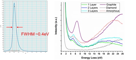
Figure 1 Left: despite the low (± 30 keV) energy of these electrons, the energy spread of the electron beam, measured by our own Hitachi EELS is 400 meV or less:. Right: EELS spectra differentiating between single , double and triple layers of graphene , graphite, diamond, and amorphous carbon.
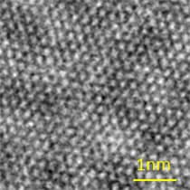
Figure 2 The low-pass-filtered BF STEM of Graphene at 30 keV shows a resolution of close to 0.2 nm; the 0.142 nm atom distances are not resolved.
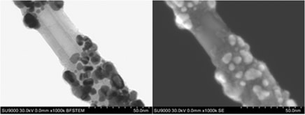
Figure 3 Left: The high-resolution 30-keV BF STEM image by itself makes it difficult to model its 3D structure. Right: Only in combination with the (simultaneously acquired) high-resolution SE image, the real structure of this sample becomes obvious and modeling this structure as a 3D model would be quite manageable.
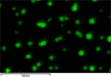
Figure 4 Elemental EDX map (Au M) at 30 kV, The size of the nano-particles is in the range of 5-10 nm. Acquisition time is 3.5 min at a current of 1 nA