- The SEM column and FIB column are orthogonally arranged to optimize the column positioning for 3D structural analysis.
- The combination of high-brightness cold-field-emission electron source and high-sensitivity optics support analysis of a wide range of materials from biological tissues to magnetic materials.
- The Micro-sampling system and Triple Beam system allow high-quality sample preparation for TEM and atom-probe applications.
Ion milling and observation at normal incidence in real-time for true analytical imaging
The SEM column and FIB column are orthogonally arranged to realize normal incident SEM imaging of FIB cross sections.
Orthogonal column arrangement eliminates aspect deformation, foreshortening of cross-sectional images, and shift of the field of view (FOV) during serial section imaging, which cannot be avoided by conventional FIB-SEM systems. The NX9000 images enable highly accurate 3D structural analysis. Optical correlative microscopy can be applied easily due to the benefit of surface-planar EM imaging.
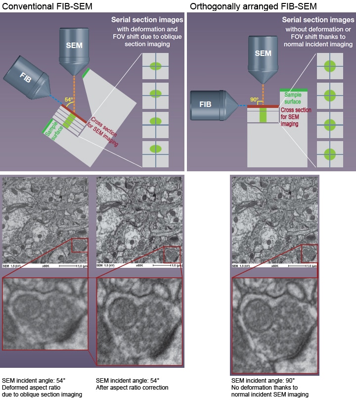
Sample: Mouse brain neuron
Sample courtesy of Yoshiyuki Kubota, Ph.D., Neural Information Processing Systems (NIPS)
Cut & See·3D-EDS*1·3D-EBSD*1 available for a wide variety of materials
Cut&See
Cut & See supports high-resolution, high-contrast imaging of biological tissues, semiconductors, and magnetic materials, such as steel and nickel, at low accelerating voltages.
Serial section images can be collected with high throughput due to the proper geometry of the ion and electron column.
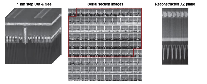
Sample: NAND flash memory
SEM accelerating voltage: 1 kV
Cutting interval: 1 nm
Number of cut: 300
3D-EDS*1
Serial section SEM images and serial section elemental maps can be collected using 3D-EDS.
The large-area silicon drift detector reduces the acquisition time and enables elemental mapping at low accelerating voltages.
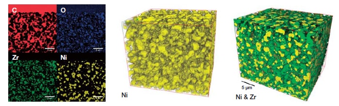
Sample: Fuel cell electrode
SEM accelerating voltage: 5 kV
Cutting interval: 100 nm
Number of cut: 212
Sample courtesy of Prof. Naoki Shikazono, University of Tokyo
3D-EBSD*1
Simultaneous SEM, FIB, and EBSD signals are obtained for 3D-EBSD without moving the stage during FIB sectioning and EBSD analysis. Accuracy and throughput of 3D crystal orientation analysis and segmentation yield high quality and less post-processing correction.
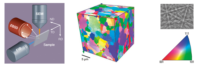
Sample: Ni
SEM accelerating voltage: 20 kV
Cutting interval: 150 nm
Number of cut: 150
- *1:
- Option
See more on Hitachi’s website
Sigmatech Inc. Philippines is the leading provider of cutting-edge laboratory equipment crucial for a wide range of applications, including Quality Assurance/Quality Control (QA/QC), Metrology, Research and Development (R&D), Failure Analysis, Environmental and Chemical Analysis, and Process Control. Serving diverse industries in the Philippines, such as Semiconductor/Electronics, Pharmaceutical, Mining, Energy, and more, we are your go-to source for top-quality equipment, including Electron Microscopes in the Philippines. About us