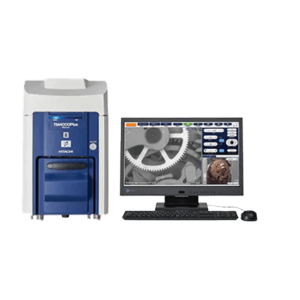
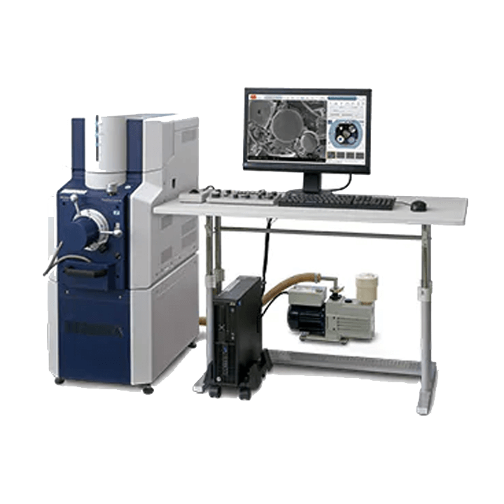
The FlexSEM 1000 II Scanning Electron Microscope features newly designed electron optical and signal detection systems providing unparalleled imaging and analytical performance in a lab-friendly configuration. Keeping efficiency in mind, the FlexSEM features an adaptable, separable, and compact design, such that it can be installed in limited office, laboratory, or even mobile spaces. Engineered to appeal to both the novice and expert microscopist for a wide range of applications, including biological and advanced material specimens, this microscope will certainly expand your analyses as well as your expectations.
Compact & High-Performance Column
Best-in-class resolution in a compact system. The FlexSEM employs a newly designed electrical optical system with a reliability-proven high-sensitivity detector, achieving imaging at 4 nm.
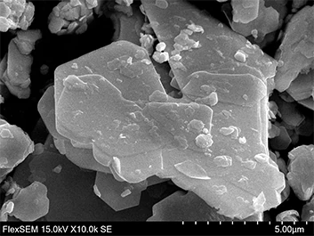
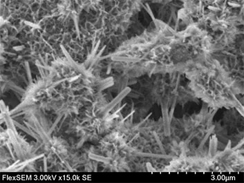
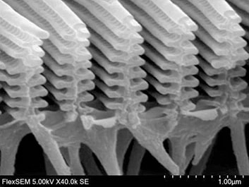
High resolution image
The electron optics incorporate a low aberration objective lens and a unique gun bias system that allows delivery of high emission current.
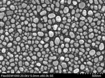
Secondary Electron (SE) Image
Magnification: 60,000X
Resolution: 4.0 nm
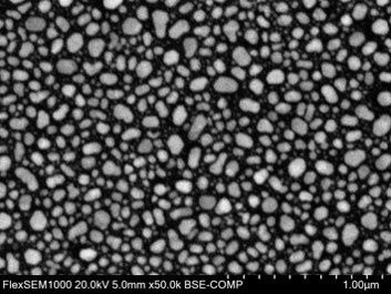
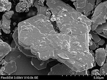
Backscattered Electron (BSE) Image
Magnification: 50,000X
Resolution: 5.0 nm
Ultra-Variable-Pressure Detector
Novel low vacuum technologies enable observation of the surface of non-conductive specimens without preprocessing, across the entire pressure and accelerating voltage ranges.
New & Improved Auto Functions
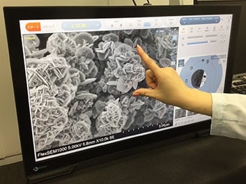
The user interface is easy to operate even by novice users, and with the various automated functions, high-quality and quick data acquisition can be accomplished regardless of user experience level. A touch panel operation is possible.
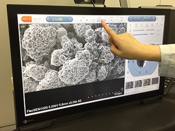
Intuitive & Correlative Navigation
SEM MAP helps to locate regions of interest quickly, and delivers accurate correlated optical and SEM images using only one click. Optical and EM correlation function, SEM MAP is fully integrated into the graphical user interface.
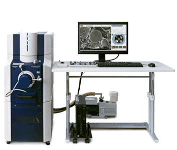
COMPACT SLIM BODY
A compact design (450 mm wide) minimizes system footprint. The FlexSEM is designed with separable units for flexible system placement. The entire system requires only a standard wall outlet for power.
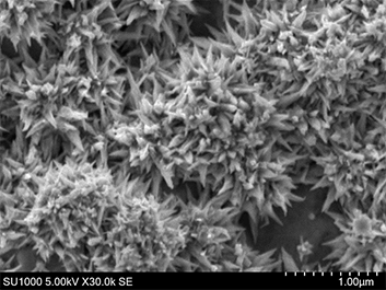
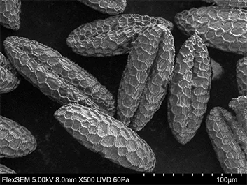
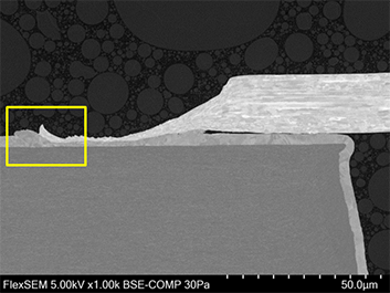
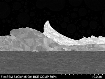
UNPARALLELED IMAGE QUALITY
The newly developed electron optical column and Ultra-Variable-Pressure Detector (UVD) enable superior imaging of specimen surfaces at low-accelerating-voltages and low-vacuum conditions.
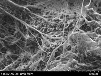
Vacc: 5 kV; Mag: 5,000X
Pressure: 50 Pa; Signal: UVD
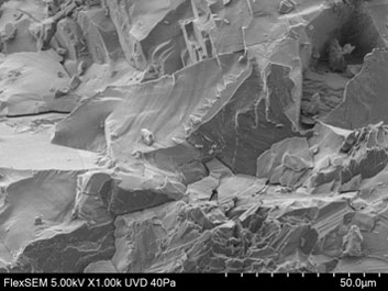
Vacc: 5 kV; Mag: 1,000X
Pressure: 40 Pa; Signal: UVD
INTUITIVE OPERATION
The user-friendly GUI as well as accurate and fast Auto Focus Control (AFC) and Auto Brightness and Contrast Control (ABCC) algorithms, take only 5 seconds to enable optimized imaging performance with minimal time and effort.
NEW CAMERA NAVIGATION – “SEM MAP”
The “SEM MAP” function makes traversing across an entire specimen effortless. Navigate your sample with the use of an optical camera, and deliver accurate correlated Optical and SEM images using only one click.
The Hitachi FlexSEM 1000 II Scanning Electron Microscope is a cutting-edge instrument designed for high-resolution imaging and analytical performance. With its compact, lab-friendly design, it features advanced electron optics and signal detection systems, achieving a resolution of 4.0 nm. Ideal for both novice and expert users, the FlexSEM 1000 II offers intuitive operation and versatile applications, making it a top choice for researchers in the Philippines


")