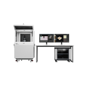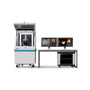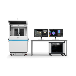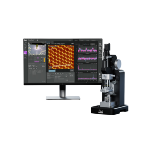
How Atomic Force Microscopy (AFM) Works
Atomic Force Microscopy, commonly known as AFM, is a nanoscale imaging and measurement technique used to examine surfaces in three dimensions. It is designed to capture highly detailed topographic images and measure surface properties at extremely small scales, even reaching atomic-level resolution. Unlike optical microscopes that rely on light, AFM works by physically sensing the surface using a very sharp probe tip. This allows the instrument to study surface features and interactions that are far smaller than what can be seen with conventional microscopy.
Understanding the Nanoscale
AFM operates in the nano world, where measurements are made in nanometers. One nanometer is one billionth of a meter. At this scale, surface behavior is strongly affected by intermolecular forces and other nanoscale interactions. These forces influence how the AFM tip responds as it moves near or across the sample surface, making AFM especially useful for studying materials at a level where surface structure and properties can directly affect performance.
Core Working Principle
At the core of AFM is a sharp tip mounted on a flexible cantilever. The tip acts like a tiny probe that scans across the sample surface. As it approaches the material, the tip begins to interact with the surface through forces such as van der Waals and electrostatic forces. These attractive forces can pull the cantilever downward. When the tip gets very close to the surface or makes contact, repulsive forces begin to dominate, pushing the cantilever upward. These extremely small movements allow the instrument to detect changes in the surface at the nanoscale.
In simple terms, AFM does not “see” the surface in the same way a camera or optical microscope does. Instead, it “feels” the surface. As the probe moves across peaks, valleys, and other surface features, the cantilever bends or deflects. The instrument records these movements and converts them into a detailed map of the surface.
How the Cantilever Movement Is Detected
To measure the movement of the cantilever, AFM uses a laser-based detection system. A laser beam is directed onto the back of the cantilever and reflected toward a position-sensitive photodetector. When the cantilever bends, even by a very small amount, the position of the reflected laser beam changes. The photodetector tracks these changes and converts them into measurable signals.
This detection method allows the AFM to monitor height variations and tip-sample interactions with very high sensitivity. The system can track surface topography and also detect different types of force interactions, including mechanical, electrical, and magnetic interactions, depending on the measurement mode being used.
Building a 3D Surface Image
As the tip scans across the sample, the AFM uses a feedback system to maintain a consistent interaction between the tip and the surface. The system continuously adjusts the position of the scanner to keep the measurement stable. By recording these adjustments and the movement of the cantilever, the AFM constructs a three-dimensional topographic map of the sample surface.
This 3D map provides detailed information about the surface, including nanoscale height variations and surface features. The technique can achieve sub-nanometer precision and can also generate quantitative data such as adhesion, stiffness, and conductivity.
AFM Imaging Modes
AFM can operate in different imaging modes depending on the sample type and the information needed. Each mode controls how the tip interacts with the surface.
Contact Mode
Contact mode is one of the most straightforward AFM methods. In this mode, the AFM tip remains in continuous contact with the sample surface while scanning. As the tip follows the surface contours, the cantilever deflects. The laser and photodetector track these deflections, while the feedback system adjusts the Z scanner to maintain a constant deflection setpoint. This allows the system to map surface topography with high sensitivity.
Contact mode is useful because it is direct, fast, and easy to understand. Since the tip stays in contact with the surface, the feedback response can be stable and rapid. However, care is needed when scanning soft or delicate materials because the constant contact force may affect or damage the sample surface.
Non-Contact Mode
In non-contact mode, the tip does not continuously touch the sample surface. Instead, the system uses attractive forces between the tip and sample for feedback. This makes it useful when the goal is to reduce physical interaction with the surface while still measuring topography and surface behavior.
Tapping Mode
Tapping mode combines aspects of contact and non-contact imaging. In this mode, the cantilever oscillates and intermittently interacts with the surface rather than dragging continuously across it. This can help reduce the effect of lateral forces while still allowing the AFM to collect topographic information. Tapping mode can also provide phase images, which may help recognize differences in sample properties.
What AFM Measures
AFM is best known for producing high-resolution 3D surface images, but its capability extends beyond simple topography. By monitoring how the tip interacts with the sample, AFM can measure or evaluate different surface-related properties. These include changes in height, adhesion, stiffness, conductivity, and other force interactions depending on the selected imaging or measurement mode.
This makes AFM a versatile technique for researchers and engineers who need more than a visual image. It provides both structural and quantitative surface information, making it useful for studying materials where nanoscale features can influence performance, reliability, or functionality.
Why AFM Is Important
The strength of AFM lies in its ability to provide detailed nanoscale information with minimal sample preparation. It can capture three-dimensional surface data and measure surface properties with high precision. This makes it valuable for studying materials that require accurate nanoscale characterization, such as thin films, advanced materials, semiconductor-related structures, polymers, coatings, and other surfaces where minute features matter.
For industries and research fields working with advanced materials, AFM offers a way to better understand how a surface is structured and how it behaves. Since many product failures, performance issues, and material differences begin at the surface or nanoscale level, AFM can provide important insights that are not always accessible through conventional imaging methods.
Summary
Atomic Force Microscopy works by scanning a surface with an extremely sharp probe tip attached to a flexible cantilever. As the tip moves near or across the sample, forces between the tip and the surface cause the cantilever to bend. A laser detection system tracks these tiny movements, and a feedback system helps maintain stable interaction between the tip and the sample. The AFM then converts the collected signals into a high-resolution 3D map of the surface, along with quantitative data about selected surface properties.
In short, AFM allows scientists and engineers to “feel” and measure surfaces at the nanoscale, revealing surface details and properties that are far beyond the reach of ordinary visual inspection.

Park Systems. (n.d.). How AFM Works – Atomic Force Microscopy. Park Systems Knowledge Center. Retrieved from https://www.parksystems.com/en/learning-center/how-afm-works
If you’re interested in an Atomic Force Microscope or looking for further information, please get in touch and a member of our team will be happy to assist.