What is surface?
A surface is the outermost layer of any physical object. It is the portion of the object that can be perceived by an observer using their sense of sight and touch and is the portion with which surrounding materials first interact. The outermost part of a material is an extremely important component responsible for interfacial characteristics such as chemical reactivity, adhesion, wetness, electrical properties, optical properties, corrosion-resistance, friction, and biocompatibility of the material.
Why is surface analysis important?
Surface analysis measurements provide a means to correlate performance with surface composition and structure. This knowledge can be used to accelerate the development of new materials or improve existing materials’ performance. The ability to characterize thin-film structures, which can be imagined as multiple discrete layers separated by interfaces provides a unique opportunity to examine the composition of materials in each layer and study interactions between them. The ability to analyze sub-micron features, defects, or particulate contaminants is of critical importance to increasing product yield in all industrial applications, including semiconductor device fabrication, hard disk read/write head and magnetic media fabrication, specialty glasses and mirrors, composite materials, renewable energy and power storage, etc.
How is surface analysis performed?
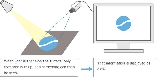
In a surface analysis, the signal from the surface is being stimulated by a primary probe such as photos, X-rays, ions, or electrons. Among the signals generated as a result of stimulation, particles such as electrons and ions are created within the top few monolayers. Their properties, including charge polarity, energy or mass, are analyzed to reveal the chemical structure of the surface.
Sometimes, information on depths from several dozen nanometers to several hundred nanometers is needed. In such cases, a depth profile analysis can be employed. Deeper layers can be examined via depth profiling, during which a beam of ions is used to remove thin layers of materials to expose deeper layers for subsequent analysis.
When performing the analysis, the solid sample is placed in a vacuum for measurement. Inside the analysis instrument, a reduced pressure state called an ultra-high vacuum, with a pressure one billionth of atmospheric pressure or lower, is created. By controlling charged particles such as X-rays, ions, and electrons, and irradiating the surface in such an environment, information on the surface’s chemical structure can be accurately detected.
Properties of three main surface analysis techniques
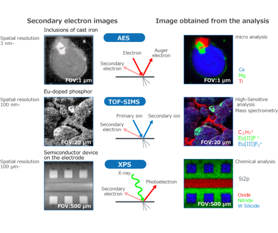
The main types of surface analysis include XPS, TOF-SIMS, and AES.
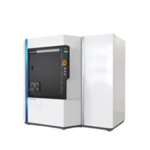
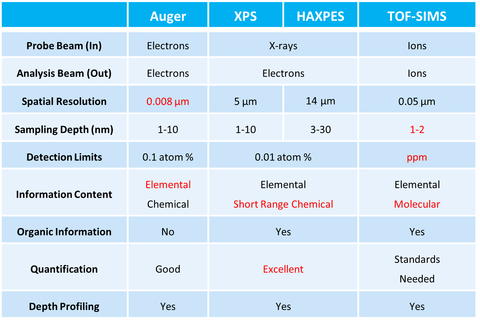
XPS is a technique in which x-rays are irradiated to analyze the energy of photoelectrons generated by the photoelectric effect. It is characterized by its ability to analyze surface compositions and chemical-bonding states. Its analysis area is limited to several microns at most, but it can be used for the surface analysis of various materials regardless of whether they are organic or inorganic.
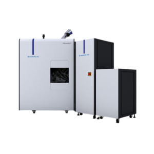
TOF-SIMS is a technique in which high-speed ions are irradiated to analyze secondary ions emitted from the surface. It is characterized by an extremely high surface sensitivity, its ability to obtain organic compound molecular mass information, and to perform high sensitivity inorganic element analysis. In the past, it was mostly used for surface metallic contamination and organic material analyses for semiconductors and display materials, while more recently it has been used for the analysis of organic matter distribution and segregation on organic material surfaces.
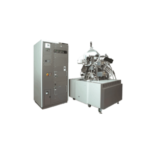
In AES, electron beams are irradiated on samples and the generated Auger electrons are observed to perform qualitative/quantitative analysis of the surface. Since the primary excitation line with AES is electrons, it can function as an electron scanning microscope. Additionally, it is characterized by extremely high spatial resolution compared to other surface analysis methods. AES demonstrates its strength mainly in the observation of metal and semiconductor surfaces and micro-level foreign substances on surfaces.
Next, let’s look at the principles and detailed characteristics of XPS, TOF-SIMS, and AES.
Common Applications
Energy
Physical Electronics XPS, AES, and SIMS surface analysis instruments are playing a critical role in understanding efficiency and lifetime issues related to energy conversion devices, energy storage devices (batteries), and many energy saving technologies.
Medical
Physical Electronics XPS and TOF-SIMS instruments are routinely used to characterize the surfaces of implantable medical devices, study the release of drugs from delivery platforms, and more recently to support basic medical research with TOF-SIMS characterization of tissue sections.
Microelectronics
Microelectronic devices typically consist of a series of thin films that have been patterned to produce a device. The use of surface analysis instruments to characterize the composition of thin films or patterned structures and detect contaminants or process residues is critical to the development of new materials, manufacturing processes, and increasing product yield.
Thin Films
Thin films and coatings are used or applied to an almost limitless range of applications to provide a specific performance characteristic for a broad range of industrial products. These include coatings that provide antistatic properties, corrosion resistance, reduce wear, and promote adhesion; as well as thin films for optical devices, mirrors, semiconductor devices, magnetic media, food wrap, etc.
Polymers
Polymeric materials are widely used for structural materials, and coatings in many research and industrial applications. Polymers are often chemically inert and require surface modification to promote properties such as adhesion and wettability. The use of PHI XPS and TOF-SIMS instruments to detect and characterize surface modification or contamination of polymer surfaces is critical to the successful end use of many polymeric materials.
Metallurgy
Corrosion and wear, and coatings to prevent corrosion and wear are often studied by XPS to provide quantitative chemical state information and by TOF-SIMS to provide molecular identification if organic materials are involved.
Content via: Physical Electronics
Physical Electronics. (n.d.). Surface Analysis Applications | Physical Electronics Inc. https://www.phi.com/surface-analysis-applications.html