Semiconductor Inspection Systems
")
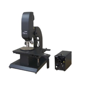
IR-2200 Microscope System enables the user to inspect sub-surface images including MEMS device, 3D stacks, incoming wafers, photovoltaic and wafer level CSP’s with an astonishing level of precision.
IR-2200 Microscope System enables the user to inspect sub-surface images including MEMS device, 3D stacks, incoming wafers, photovoltaic and wafer level CSP’s with an astonishing level of precision.

")
Seiwa Wafer review system visually inspects the defect location detected from AOI systems. This review system is able to capture the visual data and add it to previous inspection results.
Seiwa Wafer review system visually inspects the defect location detected from AOI systems. This review system is able to capture the visual data and add it to previous inspection results.
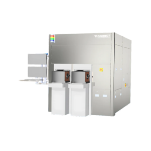
Solution for the review of defects of semiconductor integrated circuit detected by AOI/AVI at front end processing, helps to eliminate false defects and increase overall yield.
Solution for the review of defects of semiconductor integrated circuit detected by AOI/AVI at front end processing, helps to eliminate false defects and increase overall yield.
