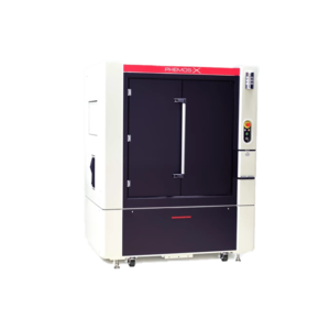
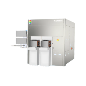
This equipment is for automated optical inspection system for semiconductor device wafers.
By using On-Fly measurement mode, system perform high speed and high accuracy
visual inspection for such as pattern defects, contamination, cracks.


This equipment is for automated optical inspection system for semiconductor device wafers.
By using On-Fly measurement mode, system perform high speed and high accuracy
visual inspection for such as pattern defects, contamination, cracks.
This equipment is for automated optical inspection system for semiconductor device wafers.
By using On-Fly measurement mode, system perform high speed and high accuracy
visual inspection for such as pattern defects, contamination, cracks.
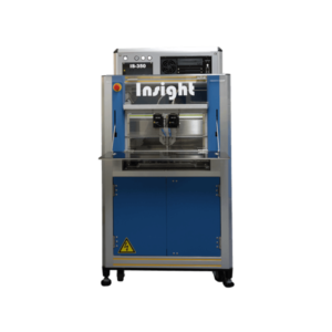
This equipment is for automated optical inspection system for semiconductor device wafers.
By using On-Fly measurement mode, system perform high speed and high accuracy
visual inspection for such as pattern defects, contamination, cracks.

")


")
")

Product added to Quote list ✔

Sign up for our newsletter to get updates on promos, seminars, events, products, application notes and more.

")


