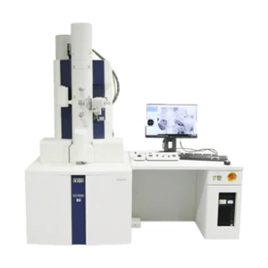
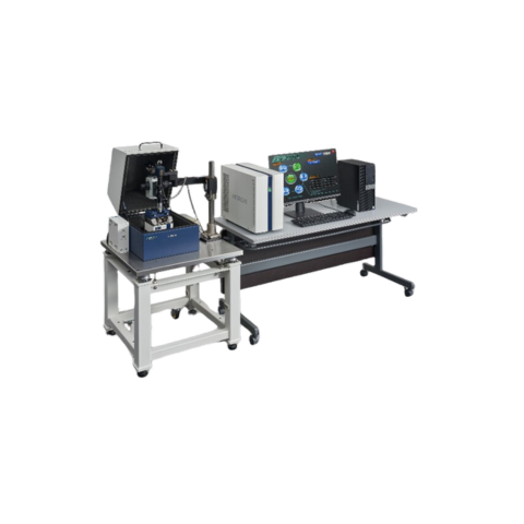
Hitachi Atomic Force Microscope AFM100 Multifunctional Probe Microscopy Platform
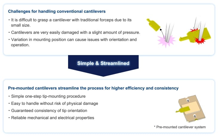
Pre-mounted cantilevers make replacement EASY(option)
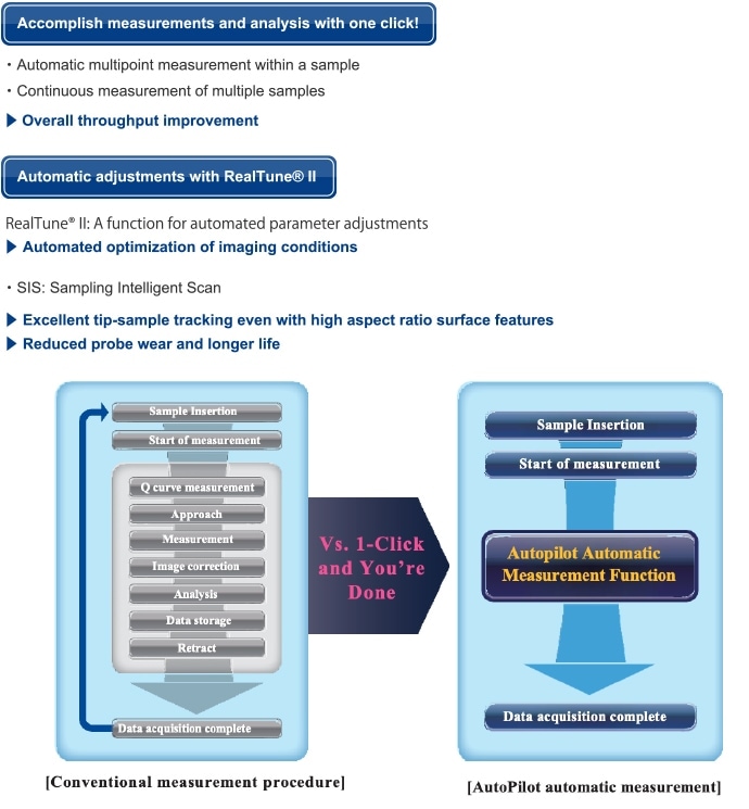
Automated measurement & analysis with one-click autopilot function
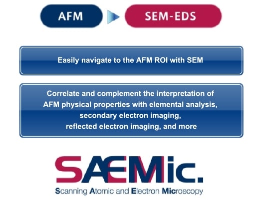
Correlative SEM-EDS Analysis with our AFM Marking Function
Analyze the same region of interest (ROI) with SEM, EDS, and AFM: More Information = Better Results!
- Automated AFM Marking Features with Navigation Software.
[Evaluating AFM-KFM-SEM-EDS of Aluminum Alloy before and after Corrosion]
![[Evaluating AFM-KFM-SEM-EDS of Aluminum Alloy before and after Corrosion]](https://www.hitachi-hightech.com/global/en/media/afm100_04_jpg_tcm27-70800.jpg)
Specifications
| AFM100 Plus | AFM100 | |
| Detection System/Light Source | Optical lever/SLD (Super luminescent diode) | |
|---|---|---|
| Lever holder | Premount holder*, multi-holder* | |
| Basic Specifications | RMS noise level: ≦0.03 nm, in-plane drift: ≦0.03 nm/sec | |
| Sample size | Max. 35 mmφ, thickness 10 mm, (max. 50 mm sq., thickness 20 mm)* | |
| Scanner (Scan range)* | (XY:20 μm/Z:1.5 μm, XY:100 μm/Z:15 μm, XY:150 μm/Z:5 μm)*(Included with a 5-year warranty) | |
| Light microscope | Microscope with zoom function (Field of view XY:1.8 x 1.38 to 0.26 x 0.2 mm)* Simple optical microscope (Field of view XY:1.6 x 1.2 mm)* | Simple optical microscope (field of view XY:1.6 × 1.2 mm) |
| Basic functions | AFM, DFM, PM, FFM, SIS-shapes/properties, Q-value control | AFM, DFM, PM, FFM, SIS-shapes |
| Vibration isolation and noise isolation mechanism | Passive vibration isolation air table and sound-proof cover | Standard tabletop |
| Sample transfer mechanism | Manual Stage XY:±2.5 mm, Impact Stage Set (Conductive Type)* | |
| Measurement environment | Atmosphere, in liquid*, heated* (room temperature to 250 °C), heated in liquid* (room temperature to 60 °C) | |
| Other functions | Self-check function, software download service, AFM marking* | |
| Power Supply Specifications | AC 100 V ± 10 V, 15 A, 1 line, D inoculated grounded receptacle | |
※The asterisk (*) in the table indicates feature is optional.
※For detailed specifications, please refer to the product specification sheet.
For more information, contact us. See more on Hitachi’s website
")
")