

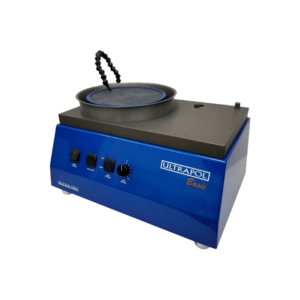
- Fully Angle adjustable – produces specific wedge angles
- Quick Release Interface allow for fast and repeatable mounting and demounting.
- Holders available for most components
- Fast process times
- Low run-out lap for flat optical polishes
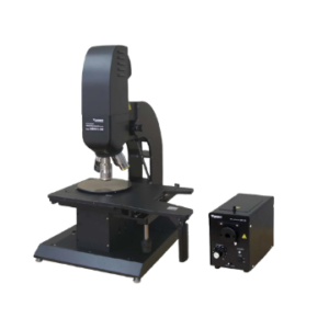
The specific workholder for an application is held firmly and repeatably with the system’s quick release interface. Standard holders are available for many applications, including:
- Capillary / glass ferrule polishing
- Planar Waveguide polishing
- Bare fiber polishing – flat and angle polishing
- Integrated optics
- Die Cross-sectioning
- SEM and TEM sample preparation
- IC Wafer and package-level backside preparation
- Encapsulated mount polishing


")
")


")
")

