The IR-2200 Infrared Microscope system integrates the infrared table top microscope system with software and 4.1 Megapixel USB-3.0 NIR Camera.
Capable of high precision measurements, image capture, verification and inspection of materials transparent to the near infrared (NIR) / Shortwave Infrared (SWIR) wavelengths.
Key Industries: Chemicals,Lenses,Semiconductor and Electronics and more.
IR-2200 Microscope System enables the user to inspect sub-surface images including MEMS device, 3D stacks, incoming wafers, photovoltaic and wafer level CSP’s with an astonishing level of precision.
IR-2200 Microscope System enables the user to inspect sub-surface images including MEMS device, 3D stacks, incoming wafers, photovoltaic and wafer level CSP’s with an astonishing level of precision.
The IM4000Plus Ion Milling System utilizes a broad, low-energy Ar+ ion beam milling method to produce wider, undistorted cross-section milling or flat milling.
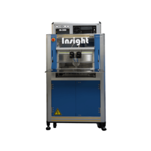
The Insight-Scan (IS) series of Scanning Acoustic Microscopes(SAM) integrates the finest state-of-the-art technology for high resolution, high speed, fully digital non-destructive sample analysis.
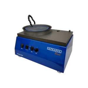
ULTRAPOL Basic lapping and polishing machine offers the build-quality required for high precision manual polishing of materials for production, research and NAND flash chip-off in digital forensics
Ultraslice Macrotome is a low-cost sectioning system designed for mobile chips, devices, and various industrial samples. This system is known for its precision and versatility.
Seiwa Wafer review system visually inspects the defect location detected from AOI systems. This review system is able to capture the visual data and add it to previous inspection results.
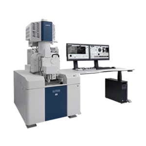
The SU8600 incorporates a highbrightness cold-field emitter (CFE) to allow acquisition of ultra-high-resolution images even at low accelerating voltages.
The ZONESEMⅡ Tabletop Sample Cleaner uses UV-based cleaning technology to minimize or eliminate hydrocarbon contamination for electron microscopy imaging.
IR-2200 Microscope System enables the user to inspect sub-surface images including MEMS device, 3D stacks, incoming wafers, photovoltaic and wafer level CSP’s with an astonishing level of precision.
ASAP-1® has become the standard preparation equipment that engineers involved in disciplines such as failure analysis, yield enhancement and competitive analysis.


")