The NEXT Generation of Innovation. Meeting and Exceeding Needs and Requirements in Many Fields.

The HT7800 RuliTEM is a 120 kV transmission electron microscope (TEM) with multiple lens configurations, including a standard lens for unsurpassed high contrast and a class-leading HR lens for high resolution.
This breakthrough in advanced innovative design allows for highly efficient workflows and many specialized applications. It represents the cutting-edge solution for modern TEM analyses.

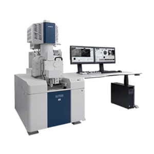
  • Hitachi’s Dual-Mode objective lens supports easy observation under low magnification, wide-field high contrast, high resolution, and more—all in one microscope.
  • Normal room light operation and automated functions allow both novice and experienced operators to use the system effectively.
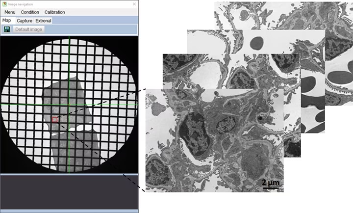
  • Advanced stage-navigation function enables whole-grid searching and efficient image acquisition.
  • Automated image stitching, 3D tomography, STEM, EDX, in-situ, and other options available for a broad range of applications.

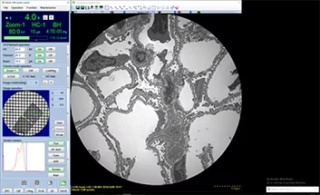
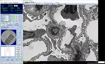
Operation under normal room light using HD screen camera

Digital functionality from beam adjustments to observation and more

Screen camera
Screen camera
Main camera
Main camera

New image navigation design for intuitive field searching

Ability to specify ROI in low-mag image and easily capture at desired magnification
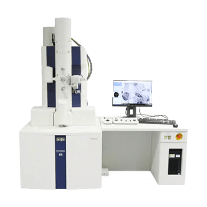
Specimen: Mouse kidney; Instrument: HT7800; Accelerating voltage: 80 kV; Direct magnification: ×2,000
Specimen: Mouse kidney
Instrument: HT7800
Accelerating voltage: 80 kV
Direct magnification: ×2,000

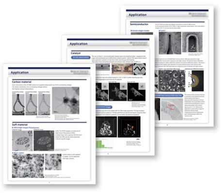
Additional functions and optional accessories

Automated Multi-frame Panoramic function, Drift Correction, Auto Pre-Irradiation, STEM, EDX, various Specimen Holders, and Electron Beam Tomography are available for a wide variety of analysis needs.

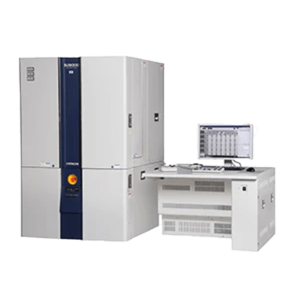
“RuliTEM” based on the Revolution of Ultimate Luxury Imaging by Hitachi HT7800 TEM
Taking transmission electron microscopy to new heights of luxury and performance

Specifications

 HT7800HT7820HT7830
Electron gunW, LaB6
Accelerating voltage20 – 120 kV (100 V/step variable)
Resolution (Lattice)0.20 nm
(Off-axis, 100 kV)
0.14 nm
(Off-axis, 120 kV)
0.14 nm
(Off-axis, 120 kV)
0.19 nm
(On-axis, 120 kV)
Maximum magnificationx600,000x800,000x1,000,000
Stage maximum tilt angle±70°±30°±10°
Standard featuresAuto focus, Microtrace, Autodrive, Live FFT display, Measurement function, Low dose, API (auto pre-irradiation), Image navigation function, Column with mild baking function, Whole view function, Drift correction function etc.

Hitachi‘s HT7800 RuliTEM is a 120 kV transmission electron microscope (TEM) with multiple lens configurations, including a standard lens for unsurpassed high contrast and a class-leading HR lens. Available through Sigmatech Inc.

Transmission Electron Microscope Philippines

The Application Data Collection has a “Life Science” section and a “Materials and Semiconductors” section, introducing typical examples of measurements and applications in each field.

Life science

Life science
Life science
  • Pathological Tissue -Dysgerminoma –
  • Pathological Tissue -Rat Alveolar Epithelium –
  • Pathological Tissue -Liver Disease –
  • Ultrafine Patterns -Rat Stomach Mucosa ‐
  • Negative staining -Adenovirus –
  • Cryo-transfer Image -Liposomes –
  • Correlative light and electron microscopy (CLEM) -Peroxisome –

Materials Science & Semiconductors

Materials Science&Semiconductors
  • Carbon material
    • Carbon nanotube
  • Soft material
    • HIPS (High Impact Polystyrene)
    • Black rubber
  • Catalyst
    • Hollow-cone dark-field observation
    • In-situ observation
    • The three-dimensional reconstruction image
  • Semiconductor
    • Silicon single crystal
    • FinFET
    • 3D NAND flash memory
Features

The Application Data Collection has a “Life Science” section and a “Materials and Semiconductors” section, introducing typical examples of measurements and applications in each field.

Life science

Life science
Life science
  • Pathological Tissue -Dysgerminoma –
  • Pathological Tissue -Rat Alveolar Epithelium –
  • Pathological Tissue -Liver Disease –
  • Ultrafine Patterns -Rat Stomach Mucosa ‐
  • Negative staining -Adenovirus –
  • Cryo-transfer Image -Liposomes –
  • Correlative light and electron microscopy (CLEM) -Peroxisome –

Materials Science & Semiconductors

Materials Science&Semiconductors
  • Carbon material
    • Carbon nanotube
  • Soft material
    • HIPS (High Impact Polystyrene)
    • Black rubber
  • Catalyst
    • Hollow-cone dark-field observation
    • In-situ observation
    • The three-dimensional reconstruction image
  • Semiconductor
    • Silicon single crystal
    • FinFET
    • 3D NAND flash memory

Related Products

Ethos offers powerful solutions integrated into a single platform including low-acceleration Ar/Xe ion-beam processing when configured as a Triple-Beam system.
The Cold Field Emission source is ideal for high-resolution imaging with a small source size and energy spread. Innovative CFE Gun technology contributes the ultimate FE-SEM with superior beam bright
With options for both oxidizing and non-oxidizing metals, as well as carbon evaporation, Quorum coaters are suitable for applications, including high-resolution SEM and FIB-SEM, ensuring precise resu
The IM4000Plus Ion Milling System utilizes a broad, low-energy Ar+ ion beam milling method to produce wider, undistorted cross-section milling or flat milling.
The Insight-Scan (IS) series of Scanning Acoustic Microscopes(SAM) integrates the finest state-of-the-art technology for high resolution, high speed, fully digital non-destructive sample analysis.
This new generation of the long-standing Hitachi tabletop microscopes (TM) integrates ease of use, optimized imaging, and high-image quality, while maintaining compact design
The AFM100 Series is Hitachi’s next generation probe microscopy platform.
PHI’s Latest Generation of TOF-SIMS, having a Modern Ergonomic Package, Smaller Footprint, and Advanced Features
The only scanning Auger nanoprobe in the world that guarantees a field emission electron source whose spatial resolution is 8 nm or less.
The MC1000 Ion Sputter Coater is a sample preparation instrument for use with a Scanning Electron Microscope (SEM) designed to deposit a thin metal coating, such as platinum (Pt), gold (Au), platinum-

How can we help?

You may contact our specialists by accomplishing form below.

failure analysis, material characterization, and metrology equipment

Subscribe to newsletter

Sign up for our newsletter to get updates on promos, seminars, events, products, application notes and more.

Inquire for this Product

Hitachi HT7800
Transmission Electron Microscope (TEM)
Hitachi HT7800
Transmission Electron Microscope (TEM)