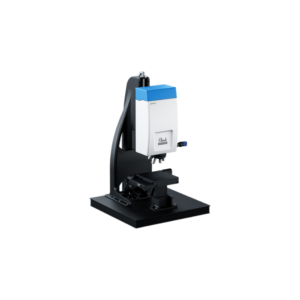
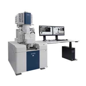
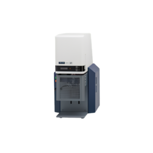
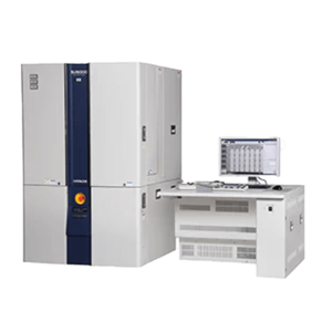
The PHEMOS-X is a high-resolution emission microscope that pinpoints failure locations in semiconductor devices by detecting the weak light emissions and heat emissions caused by defects. Available in Philippines through Sigmatech Inc.
Two ultra-high sensitivity cameras are mountable
Coverage of different detection wavelength ranges for emission analysis and thermal analysis allows easy selection of an analysis technique that matches the sample and failure mode.
Up to 7 light sources for OBIRCH, DALS, EOP and laser marker are mountable
High accuracy stage designed for advanced devices
Working range of optical stage
| X | ±20 mm |
|---|---|
| Y | ±20 mm |
| Z | +80 mm |
* Working range might be narrower than these values due to the prober being used and interference with the sample stage or mounting of a NanoLens.
Basic display functions
Superimposed display/contrast enhancement function

* The actual display may differ depending on your software version, environment, etc.
The PHEMOS-X superimposes the emission image on a high-resolution pattern image to localize defect points quickly.
The contrast enhancement function makes an image clearer and more detailed.
Display function
- Annotations: Comments, arrows, and other indicators can be displayed on an image at any location desired.
- Scale display: The scale width can be displayed on the image using segments.
- Grid display: Vertical and horizontal grid lines can be displayed on the image.
- Thumbnail display: Images can be stored and recalled as thumbnails, and image information such as stage coordinates can be displayed.
- Split screen display: Pattern images, emission images, superimposed images, and reference images can be displayed in a 6-window screen at once.
Example of connection to the LSI tester

As devices become more complicated, there is increased demand for analysis under an LSI tester connection to find a failure occurring at a specific point while a device is functioning. It is possible to connect an LSI tester with the PHEMOS-X by a short cable and using a probe card adapter specifically designed for the analysis under the PHEMOS-X optics.
Specifications
| Dimensions/Weights | Main unit: 1656 mm (W) × 2000 mm (H) × 1247 mm (D), Approx. 1640 kg Operation desk*1: 1000 mm (W) × 700 mm (H) × 800 mm (D) Approx. 39.2 kg (C16216-01 Operation desk) / 1480 mm (W) × 700 mm (H) × 800 mm (D) Approx. 48.6 kg (C16216-02 Operation desk) |
|---|---|
| Line voltage | Single phase 200 V to 240 V |
| Power consumption | Approx. 3300 VA |
| Vacuum | 80 kPa or more |
| Compressed air*2 | 0.6 MPa to 0.7 MPa |
*1: Option
*2: Including a regulator