
Semiconductor devices power nearly every aspect of modern technology, from smartphones and computers to medical equipment, automotive electronics, and industrial automation systems. As integrated circuits continue to become smaller and more densely packed, even microscopic defects can affect device performance, reliability, and manufacturing yield.
When an electronic component fails, identifying the exact cause of failure is essential for improving product quality and preventing similar issues in future production. This process, known as semiconductor failure analysis, enables engineers to locate hidden defects, evaluate manufacturing processes, and optimize device performance before products reach the market.
Traditional inspection techniques often struggle to locate electrical defects buried deep within advanced semiconductor devices. Modern failure analysis systems overcome this challenge by using specialized imaging technologies that detect extremely weak light emissions generated by defective circuits while the device is operating.
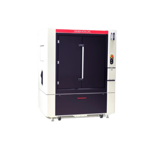
One of the most widely used technologies for this purpose is emission microscopy. Systems such as the Hamamatsu PHEMOS-X Emission Microscope provide engineers with a fast, non-destructive method for locating failure sites with high accuracy, supporting semiconductor manufacturers throughout product development, quality assurance, and reliability testing.
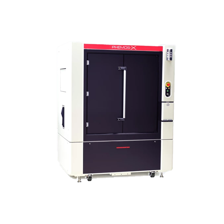
The Hamamatsu PHEMOS-X Emission Microscope enables high-resolution semiconductor failure analysis by detecting weak light emissions generated by defective integrated circuits.
What Is Semiconductor Failure Analysis?
Semiconductor failure analysis is the process of investigating integrated circuits and electronic devices to determine the cause of electrical or physical failures. The goal is to identify defects quickly so manufacturers can improve production processes, increase device reliability, and reduce manufacturing costs.
Failure analysis is commonly performed during:
- Semiconductor manufacturing
- Product development
- Reliability testing
- Quality assurance
- Root cause investigation
- Device qualification
By locating failure points early, manufacturers can reduce production losses and improve overall product quality.
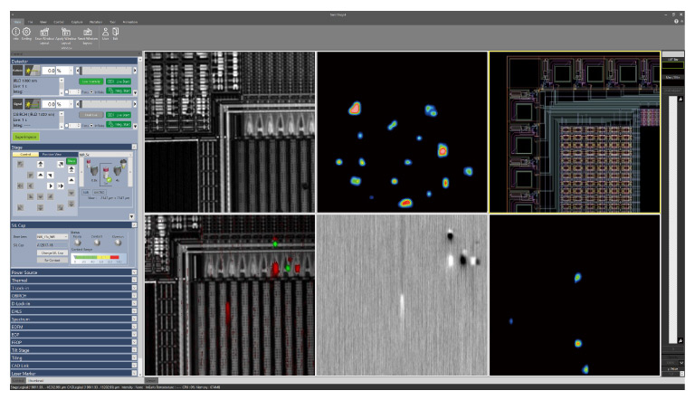
The PHEMOS-X overlays emission images with high-resolution optical images, allowing engineers to identify defect locations more quickly and accurately.
How the Hamamatsu PHEMOS-X Supports Failure Analysis
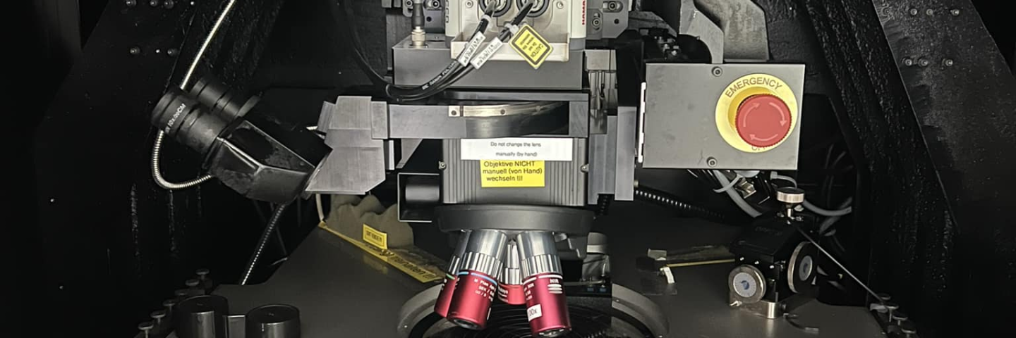
The Hamamatsu PHEMOS-X is a high-resolution emission microscope designed specifically for semiconductor failure analysis. It detects weak light and heat emissions produced by defective circuits while electronic devices are operating, enabling engineers to pinpoint failure locations without damaging the sample.
The system supports visible and near-infrared analysis through multiple light sources and ultra-high sensitivity cameras, allowing users to select the most appropriate analysis method based on the device structure and failure mode. Advanced imaging functions such as superimposed image display and contrast enhancement help simplify defect localization and improve analytical efficiency.
Because the PHEMOS-X performs non-destructive analysis, engineers can continue with additional electrical or physical investigations after locating the defect, making it an essential tool for advanced semiconductor laboratories.
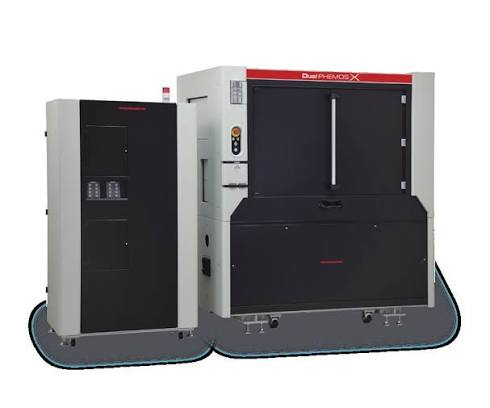
The PHEMOS-X can be connected to an LSI tester, enabling engineers to analyze semiconductor failures while devices are operating under real testing conditions.
Applications Across Different Industries
The Hamamatsu PHEMOS-X supports failure analysis and quality improvement across a wide range of industries, including:
- Semiconductor manufacturing
- Integrated circuit (IC) development
- Automotive electronics
- Consumer electronics
- Research and development laboratories
- University research facilities
- Reliability and quality assurance laboratories
Its ability to perform accurate, non-destructive defect localization makes it a valuable solution for organizations developing increasingly complex semiconductor technologies.