
")
")


Advanced Semiconductor Failure Analysis with Hamamatsu Emission Microscopes
Introduction
In the semiconductor industry, ensuring the reliability and performance of devices is crucial. Hamamatsu Photonics offers advanced failure analysis systems designed to identify and analyze defects in semiconductor devices. These systems are essential for maintaining high standards of quality and reliability in semiconductor manufacturing.
What is Failure Analysis?
Failure analysis is the process of investigating and identifying the causes of failure in semiconductor devices. This involves detecting and analyzing defects that can affect the performance and reliability of the devices. Failure analysis is critical for improving manufacturing processes and ensuring the quality of semiconductor products.
The Semiconductor Manufacturing Process: Why Failure Analysis Matters
Semiconductor fabrication involves hundreds of intricate steps—lithography, doping, etching, deposition, and packaging—each of which can introduce potential defects. Even a microscopic imperfection can lead to catastrophic failure in high-performance applications such as automotive electronics, telecommunications, and consumer devices. Failure analysis tools like emission microscopes are indispensable for: Identifying latent defects in advanced nodes (e.g., 7nm, 5nm, and below), validating process integrity during R&D and production, supporting yield improvement and quality assurance, and enabling root cause analysis for field returns and reliability testing.
Hamamatsu’s failure analysis systems utilize advanced imaging and detection technologies to pinpoint defects in semiconductor devices. The process involves several key steps:
Sample Preparation: The semiconductor device is prepared for analysis, which may involve decapsulation or cross-sectioning.
Imaging: High-resolution imaging techniques, such as emission microscopy, are used to detect light and heat emissions from defects.
Signal Detection: Various signals, including photoemission and thermal signals, are detected and analyzed to locate and characterize defects.
Data Analysis: The collected data is analyzed to determine the nature and cause of the defects.
Hamamatsu Failure Analysis Systems
Hamamatsu offers a range of failure analysis systems designed to meet the needs of semiconductor manufacturers. Some notable models include:
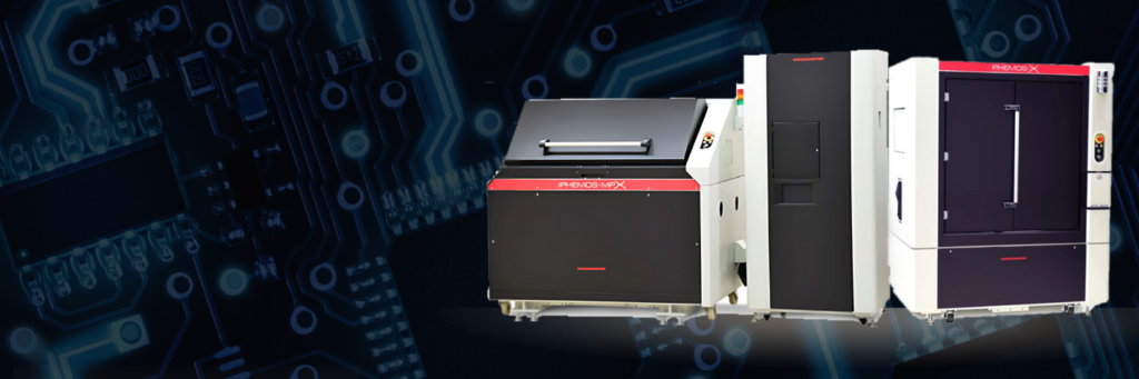
- iPHEMOS-MPX: An inverted emission microscope that detects weak light emissions and heat emissions caused by defects. It supports both static and dynamic analysis, making it suitable for a wide range of applications.
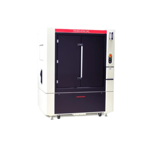
- PHEMOS-X: A high-resolution emission microscope that pinpoints failure locations by detecting light and heat emissions. It is designed for advanced, 3D, nontransparent devices and supports simultaneous optical failure analysis from both sides (top and bottom) at the wafer or die level.
- Dual PHEMOS-X: This model allows for failure analysis from both sides of a device, making it ideal for complex, 3D semiconductor devices. It features a high-accuracy stage and multiple detectors for various analysis methods.
Hamamatsu’s failure analysis systems are used in a variety of applications, including:
- Semiconductor Manufacturing: Identifying and analyzing defects in semiconductor devices to improve manufacturing processes.
- Quality Control: Ensuring the reliability and performance of semiconductor products.
- Research and Development: Investigating new materials and processes for semiconductor manufacturing.
Advantages of Using Hamamatsu
- High Resolution: These systems provide high-resolution imaging to detect even the smallest defects.
- Advanced Detection: Capable of detecting both light and heat emissions, providing comprehensive analysis of defects.
- Versatility: Suitable for a wide range of semiconductor devices and applications.
Conclusion
Hamamatsu failure analysis systems are essential tools for the semiconductor industry, offering advanced imaging and detection capabilities to ensure the reliability and performance of semiconductor devices. By utilizing these systems, manufacturers can improve their processes, enhance product quality, and drive innovation in semiconductor technology.
Keywords: Failure analysis, Hamamatsu failure analysis systems, iPHEMOS-MPX, PHEMOS-X, Dual PHEMOS-X, semiconductor defects, semiconductor reliability, high-resolution imaging, semiconductor manufacturing, Lab equipment Philippines.
