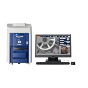
The Future of Tabletop Microscopes is Here!

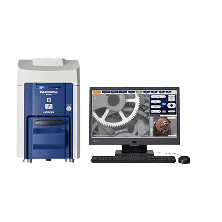
The TM4000 Series features innovation and cutting-edge technologies which redefine the capabilities of a tabletop microscope. This new generation of the long-standing Hitachi tabletop microscopes (TM) integrates ease of use, optimized imaging, and high-image quality, while maintaining the compact design of the well-established Hitachi TM Series products. Experience the new dimension of tabletop microscopes with the Hitachi TM4000 II and TM4000Plus II.

Key Industries: Chemicals, Mining, Polymers, Semiconductor and Electronics and more.

Tabletop Scanning Electron Microscope Philippines

The Hitachi TM4000II and TM4000Plus II Scanning Electron Microscopes (SEM) offer advanced imaging capabilities with user-friendly operation. These tabletop SEMs provide high-resolution images and elemental analysis, making them ideal for research, quality control, and educational applications. Available in the Philippines through Sigmatech Inc.
Tabletop Scanning Electron Microscope Philippines

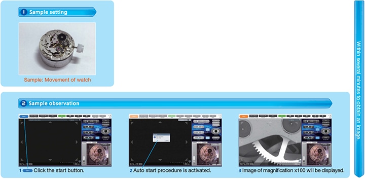
A quality image can be obtained with simple steps.
-

Automation, Observation, and Elemental Analysis

Easy to switch images with one-click.

-

Rapid acquisition of elemental maps *2

-

Sample : Movement of watch

*1Secondary electron images and MIX images can only be observed in TM4000Plus II

*2Option

Intuitive operation on Camera Navi *

Use of optical images helps navigate to target observation area easily.
Obtained SEM images can be layered on a SEM MAP image.

-

Sample: Movement of watch

*Option: Camera Navigation System

Report Creator

Simply select images and a template to create a customized reports.
Created reports can be saved/edited in Microsoft Office® formats.

-

Sample : Movement of watch

The image on the screen includes options.

Various imaging applications using 4-under low vacuum status.

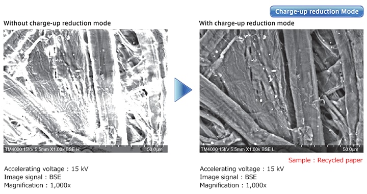
Charge-up reduction mode

Charge on a sample can be reduced by one-click.
-

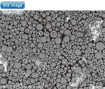
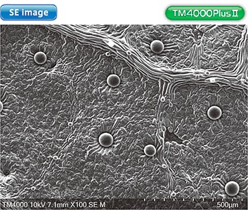
Image a variety of materials under low vacuum condition

The images show observations of non-conductive samples such as ink toner particles and a hydrated leaf surface.
-
Sample: Paint ink
Accelerating voltage: 5 kV
Image signal: BSE
Magnification: 2,500x
-
Sample: Leaf of plant
Accelerating voltage: 10 kV
Image signal: SE
Magnification: 100x

Various imaging applications using 4-under low vacuum status.

Innovative secondary-election detector to obtain surface detail with non-conductive samples at lower vacuum conditions

The TM4000Plus II can observe not only conductive samples, but also non-conductive or hydrated samples without sample preparation. Switching between BSE and SE can be performed easily.

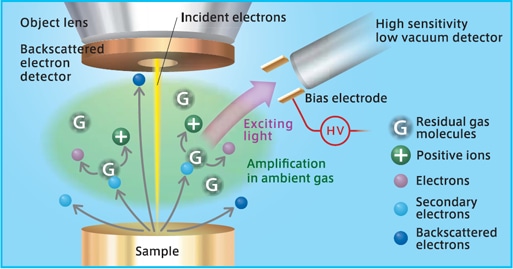
High-sensitivity Low vacuum SE Detector (UVD)

Hitachi’s UVD generates secondary-electron images by detecting visible light excited by electron gas interactions.
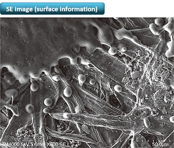
-
-
Accelerating voltage: 5 kV
Image signal: SE
Magnification: 800x
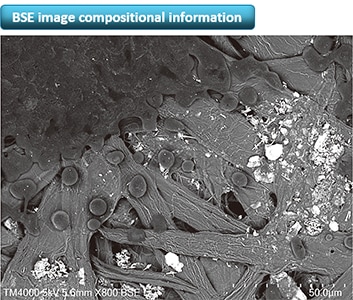
-
Sample: Printed paper
Accelerating voltage: 5 kV
Image signal: BSE
Magnification: 800x

Advantages of 20 kV accelerating voltage

High accelerating voltage enables higher-speed EDS analysis.

EDS mapping data at 20 kV in 2 min
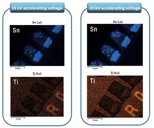
-
Sample: Electronic components

Multi Zigzag (Option)

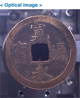
A function that takes multiple high-magnification images and stitches them together to create a single high-resolution image.
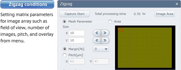
-
-
-
Sample: Japanese ancient coin
Accelerating voltage: 15 kV
Image signal: SE
Magnification: 30x
Field of view 10 vertically × 12
horizontally
(some parts were trimmed)

STEM holder (Option)

Easily obtain transmitted images on thin samples

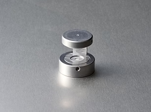
The newly developed STEM holder can be used to perform transmission images with the Hitachi UVD. Images of thin or biological samples can be obtained.

-

*UVD is a function of TM4000Plus II.

-
-
Sample : Abrasive
Accelerating voltage : 20 kV
Image signal : (a) STEM, (b) BSE
Magnification : 10,000 x
-
-
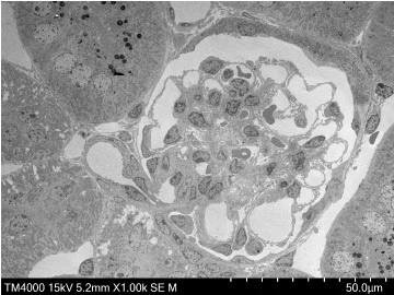
Sample : Rat kidney
Accelerating voltage : 15 kV
Image signal : STEM
Magnification : 1,000 x
-
Sample : Rat liver
Accelerating voltage : 15 kV
Image signal : STEM
Magnification : 5,000 x Specifications Model name TM4000Plus II TM4000 II Magnifications 10× – 100,000× (Photographic magnification)
25× – 250,000× (monitor display magnification) Accelerating voltage 5 kV, 10 kV, 15 kV, 20 kV Image signal Backscattered electron
Secondary electron
Mix (Backscattered electron + Secondary electron) Backscattered electron Vacuum mode BSE: Conductor/Standard/Charge-up reduction
SE: Standard/Charge-up reduction
Mix: Standard/Charge-up reduction BSE: Standard/Charge-up reduction Sample stage traverse X: 40 mm, Y: 35 mm Maximum sample size 80 mm (diameter), 50 mm (thickness) Electron gun Pre-centered cartridge tungsten filament Signal detection system High-Sensitivity 4-segment BSE detector
High-Sensitivity Low-Vacuum SE detector (UVD) High-Sensitivity 4-segment BSE detector Evacuation system
(vacuum pump) Turbo molecular pump : 67 L/s×1 unit
Diaphragm pump : 20 L/min×1 unit Size / weight Main unit (motorized stage): 330 (width)×614 (depth)×547 (height) mm, 54 kg
Main unit (manual stage): 330(width)×617(depth)×547(height) mm, 54 kg
Diaphragm pump: 144 (width)×270 (depth)×216 (height) mm, 5.5kg

Features

A quality image can be obtained with simple steps.

-

Automation, Observation, and Elemental Analysis

Easy to switch images with one-click.

-

Rapid acquisition of elemental maps *2

-

Sample : Movement of watch

*1Secondary electron images and MIX images can only be observed in TM4000Plus II

*2Option

Intuitive operation on Camera Navi *

Use of optical images helps navigate to target observation area easily.
Obtained SEM images can be layered on a SEM MAP image.

-

Sample: Movement of watch

*Option: Camera Navigation System

Report Creator

Simply select images and a template to create a customized reports.
Created reports can be saved/edited in Microsoft Office® formats.

-

Sample : Movement of watch

The image on the screen includes options.

Various imaging applications using 4-under low vacuum status.

Charge-up reduction mode

Charge on a sample can be reduced by one-click.

-

Image a variety of materials under low vacuum condition

The images show observations of non-conductive samples such as ink toner particles and a hydrated leaf surface.

-
Sample: Paint ink
Accelerating voltage: 5 kV
Image signal: BSE
Magnification: 2,500x
-
Sample: Leaf of plant
Accelerating voltage: 10 kV
Image signal: SE
Magnification: 100x

Various imaging applications using 4-under low vacuum status.

Innovative secondary-election detector to obtain surface detail with non-conductive samples at lower vacuum conditions

The TM4000Plus II can observe not only conductive samples, but also non-conductive or hydrated samples without sample preparation. Switching between BSE and SE can be performed easily.

High-sensitivity Low vacuum SE Detector (UVD)

Hitachi’s UVD generates secondary-electron images by detecting visible light excited by electron gas interactions.

-
-
Accelerating voltage: 5 kV
Image signal: SE
Magnification: 800x
-
Sample: Printed paper
Accelerating voltage: 5 kV
Image signal: BSE
Magnification: 800x

Advantages of 20 kV accelerating voltage

High accelerating voltage enables higher-speed EDS analysis.

EDS mapping data at 20 kV in 2 min

-
Sample: Electronic components

Multi Zigzag (Option)

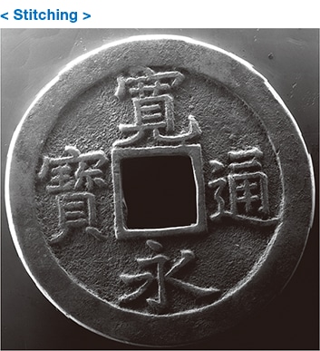
A function that takes multiple high-magnification images and stitches them together to create a single high-resolution image.
-
-
-
Sample: Japanese ancient coin
Accelerating voltage: 15 kV
Image signal: SE
Magnification: 30x
Field of view 10 vertically × 12
horizontally
(some parts were trimmed)

STEM holder (Option)

Easily obtain transmitted images on thin samples

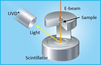
The newly developed STEM holder can be used to perform transmission images with the Hitachi UVD. Images of thin or biological samples can be obtained.
-

*UVD is a function of TM4000Plus II.
-
-
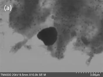
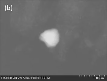
Sample : Abrasive
Accelerating voltage : 20 kV
Image signal : (a) STEM, (b) BSE
Magnification : 10,000 x
-
-
Sample : Rat kidney
Accelerating voltage : 15 kV
Image signal : STEM
Magnification : 1,000 x
-
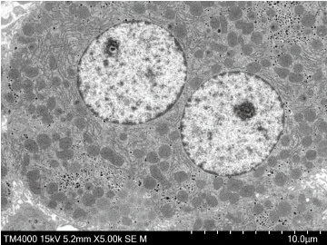
Sample : Rat liver
Accelerating voltage : 15 kV
Image signal : STEM
Magnification : 5,000 x

Specifications

Model name TM4000Plus II TM4000 II
Magnifications 10× – 100,000× (Photographic magnification)
25× – 250,000× (monitor display magnification)
Accelerating voltage 5 kV, 10 kV, 15 kV, 20 kV
Image signal Backscattered electron
Secondary electron
Mix (Backscattered electron + Secondary electron)
Backscattered electron
Vacuum mode BSE: Conductor/Standard/Charge-up reduction
SE: Standard/Charge-up reduction
Mix: Standard/Charge-up reduction
BSE: Standard/Charge-up reduction
Sample stage traverse X: 40 mm, Y: 35 mm
Maximum sample size 80 mm (diameter), 50 mm (thickness)
Electron gun Pre-centered cartridge tungsten filament
Signal detection system High-Sensitivity 4-segment BSE detector
High-Sensitivity Low-Vacuum SE detector (UVD)
High-Sensitivity 4-segment BSE detector
Evacuation system
(vacuum pump)
Turbo molecular pump : 67 L/s×1 unit
Diaphragm pump : 20 L/min×1 unit
Size / weight Main unit (motorized stage): 330 (width)×614 (depth)×547 (height) mm, 54 kg
Main unit (manual stage): 330(width)×617(depth)×547(height) mm, 54 kg
Diaphragm pump: 144 (width)×270 (depth)×216 (height) mm, 5.5kg

Related Products

IR-2200 Microscope System enables the user to inspect sub-surface images including MEMS device, 3D stacks, incoming wafers, photovoltaic and wafer level CSP’s with an astonishing level of precision.
Hitachi’s DMA is the perfect tool for assessing both stiff and soft samples, while also capturing rapid modulus changes.
The IS-202 Scanning Acoustic Microscope combines highest resolution with a very compact mechanical set-up.
The only scanning Auger nanoprobe in the world that guarantees a field emission electron source whose spatial resolution is 8 nm or less.
PHI’s Latest Generation of TOF-SIMS, having a Modern Ergonomic Package, Smaller Footprint, and Advanced Features
The iPHEMOS-MPX is a high-resolution Inverted Emission Microscope that pinpoints failure locations in semiconductor devices by detecting the weak light emissions and heat emissions caused by defects.
With options for both oxidizing and non-oxidizing metals, as well as carbon evaporation, Quorum coaters are suitable for applications, including high-resolution SEM and FIB-SEM, ensuring precise resu
Seiwa Wafer review system visually inspects the defect location detected from AOI systems. This review system is able to capture the visual data and add it to previous inspection results.
This new generation of the long-standing Hitachi tabletop microscopes (TM) integrates ease of use, optimized imaging, and high-image quality, while maintaining compact design
DSC is used to measure heat flow for material characterization by providing thermal properties such as melting point, glass transition and crystallization.

How can we help?

You may contact our specialists by accomplishing form below.

Website menu

Download catalog

To download e-catalog, please submit your details below.

failure analysis, material characterization, and metrology equipment

Subscribe to newsletter

Sign up for our newsletter to get updates on promos, seminars, events, products, application notes and more.

Inquire for this Product

TM4000 Plus
Tabletop Scanning Electron Microscope
TM4000 Plus
Tabletop Scanning Electron Microscope