


Understanding Scanning Electron Microscopes
Introduction
In the realm of advanced microscopy, Scanning Electron Microscopes (SEM) stand out as a powerful tool for detailed imaging and analysis. Whether you’re in materials science, biology, or industrial research, understanding how SEMs work and their applications can be incredibly beneficial.
What is a Scanning Electron Microscope (SEM)?
A Scanning Electron Microscope (SEM) is a type of electron microscope that produces high-resolution images of a sample by scanning its surface with a focused beam of electrons. Unlike traditional light microscopes, SEMs use electrons instead of light to form an image, allowing for much higher magnification and resolution.
How Does a Scanning Electron Microscope Work?
The working principle of an SEM involves several key steps:
- Electron Beam Generation: An electron gun generates a beam of electrons.
- Beam Focusing: Electromagnetic lenses focus the electron beam onto the sample.
- Scanning: The focused beam scans the sample in a raster pattern.
- Interaction and Signal Detection: As the electrons interact with the atoms in the sample, various signals are produced, including secondary electrons, backscattered electrons, and characteristic X-rays.
- Image Formation: Detectors collect these signals and convert them into an image, revealing detailed information about the sample’s surface topography and composition2.
Typical types of Scanning Electron Microscopes
There are various types of SEMs designed to meet different needs:
- Tabletop SEMs: Compact and user-friendly, ideal for educational purposes and small-scale research.
- Benchtop SEMs: Slightly larger than tabletop models, offering higher resolution and more advanced features.
- Floor Model SEMs: Large, high-performance instruments used in advanced research and industrial applications1.
- Environmental SEMs (ESEM): Capable of imaging wet or non-conductive samples without extensive preparation2.
Attachments and Enhancements
SEMs can be equipped with various attachments to enhance their capabilities including:
- Energy Dispersive X-ray Spectroscopy (EDX): Allows for elemental analysis by detecting characteristic X-rays emitted from the sample.
- Electron Backscatter Diffraction (EBSD): Provides crystallographic information by analyzing backscattered electrons.
- Cathodoluminescence (CL): Used to study optical properties by detecting photons emitted from the sample3.
Applications of Scanning Electron Microscopes
SEMs are used in a wide range of applications, including:
- Materials Science: Analyzing the microstructure of metals, ceramics, and composites.
- Biology: Examining the surface morphology of cells and tissues.
- Semiconductor Industry: Inspecting the quality and structure of semiconductor devices.
- Forensics: Investigating evidence at a microscopic level.
- Nanotechnology: Studying nanomaterials and nanostructures2.
Advantages of Using SEMs
- High Resolution: SEMs can achieve resolutions better than 1 nanometer.
- Depth of Field: They provide a greater depth of field compared to light microscopes.
- Versatility: SEMs can be used to study a wide variety of samples, from biological specimens to industrial materials1.
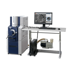
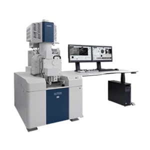
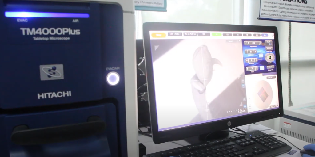
Hitachi Scanning Electron Microscopes
Hitachi offers a range of SEMs known for their innovative electron optics and signal detection systems. Some notable models include:
- SU3800/SU3900: These models deliver both operability and expandability, with the SU3900 featuring a large multipurpose specimen chamber.
- FlexSEM 1000 II: A compact model with a thermionic electron source, achieving a resolution of 4.0nm. It also offers a low vacuum mode for rapid observation of non-conductive samples.
- SU5000: This Schottky Field Emission SEM features the EM Wizard, a knowledge-based system for SEM imaging that simplifies operation and enhances imaging quality.
- SU8600: An ultrahigh-resolution cold-field emission SEM that incorporates multifaceted imaging, automation, and increased system stability, making it suitable for advanced research.
Conclusion
The Scanning Electron Microscope is an indispensable tool in modern science and industry. Its ability to provide detailed images at high resolutions makes it invaluable for research and development. Companies like Sigmatech Inc. continue to support scientific advancement by offering state-of-the-art SEM technology from Hitachi. Whether you’re a researcher, educator, or industry professional, understanding and utilizing SEMs can significantly enhance your work.
Keywords: Scanning Electron Microscope, SEM, Scanning Electron Microscope Philippines, Sigmatech Inc., high-resolution imaging, electron microscopy, Hitachi TM4000II, materials science, nanotechnology, biological imaging.
