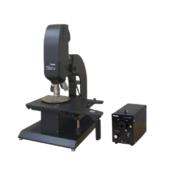
IR-2200 Microscope System enables the user to inspect sub-surface images including MEMS device, 3D stacks, incoming wafers, photovoltaic and wafer level CSP’s with an astonishing level of precision.
The IR-2200 Infrared Microscope system integrates the infrared table top microscope system with software and 4.1 Megapixel USB-3.0 NIR Camera.
Capable of high precision measurements, image capture, verification and inspection of materials transparent to the near infrared (NIR) / Shortwave Infrared (SWIR) wavelengths.
High end Seiwa NIR microscope for observing inside of semiconductor devices such as wafers, chips, MEMs and CSPs using characteristics of infrared light.
- Able to observe wavelength of up to 1550nm, providing high contrast images compared to existing microscopes which can observe up to 1100nm.
- Manual XY stage (Size 125mm x 125mm / Moving distance=±25mm ).
- Koehler coaxial illumination port.
- Objective lens with high transmittance %, focal length = 200mm.
- Built in image processing software to further provide clarity to image


")
")


")
")