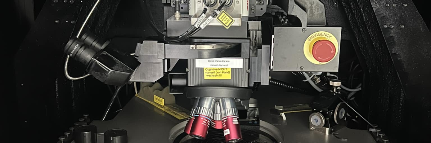
Modern manufacturing and research depend on accurate material characterization to ensure product quality, reliability, and performance. Even microscopic defects such as cracks, contamination, coating failures, or particle inconsistencies can affect the durability and functionality of a product. To detect these issues before they become costly problems, laboratories rely on Scanning Electron Microscopy (SEM) as a powerful analytical tool for detailed material evaluation.
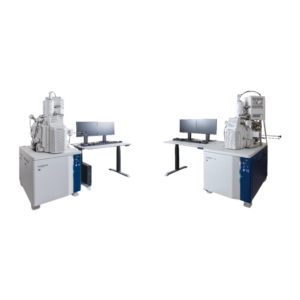
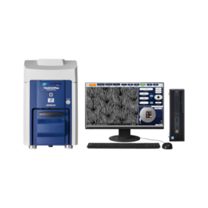
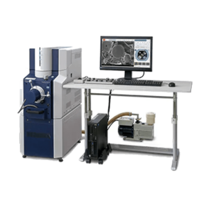
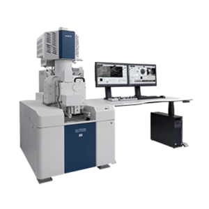
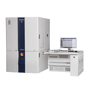
Today, SEM is used in universities, research institutions, semiconductor manufacturing, metallurgy, life sciences, and industrial quality control. Compact systems such as the Hitachi High-Tech FlexSEM 1000 II make advanced electron microscopy more accessible by combining high-resolution imaging, intuitive operation, and a space-saving design suitable for modern laboratories.
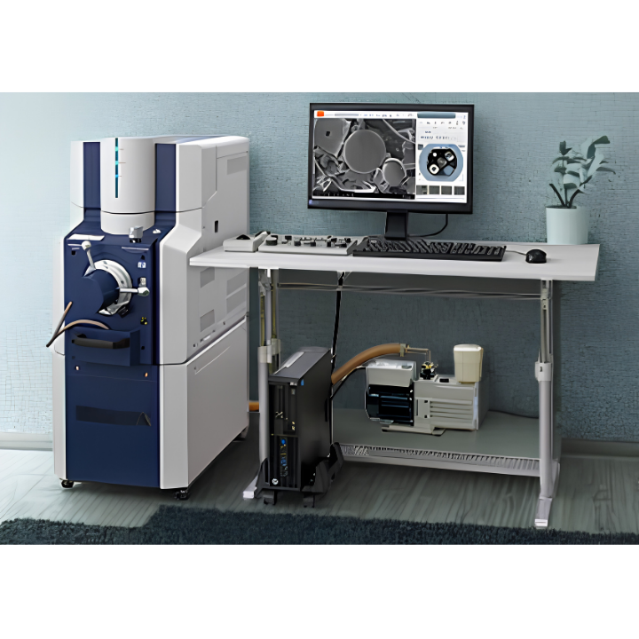
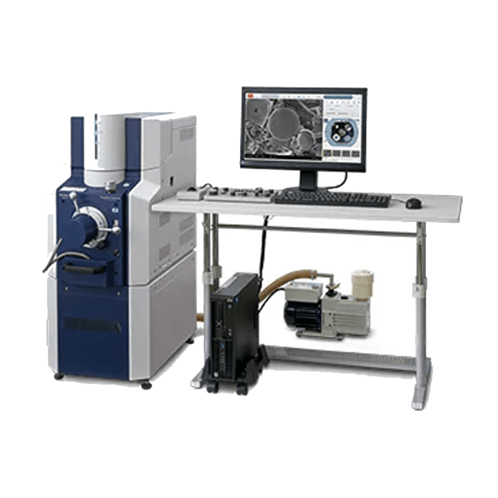
The Hitachi High-Tech FlexSEM 1000 II delivers high-resolution scanning electron microscopy in a compact and user-friendly platform suitable for research and industrial laboratories.
Why Use a Scanning Electron Microscope?
If you’re new to electron microscopy, read our guide on What is a Scanning Electron Microscope (SEM)? to understand how the technology works before exploring its industrial applications.
Researchers use SEM to examine:
- Surface morphology and texture
- Microstructural defects
- Particle size and shape
- Coating thickness
- Fracture surfaces
- Material contamination
- Biological specimens
- Electronic components
These analyses provide valuable information for product development, process optimization, failure investigations, and routine quality assurance across multiple industries.
These detailed observations help scientists and engineers understand material properties, investigate product failures, and improve manufacturing processes.
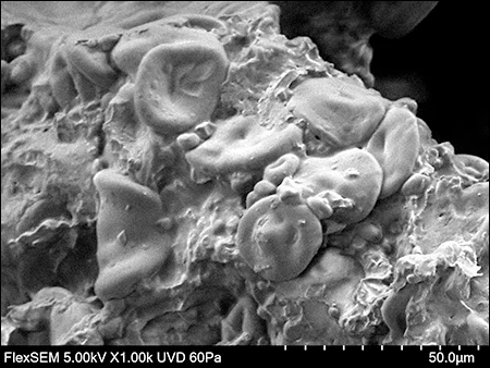
How the Hitachi High-Tech FlexSEM 1000 II Supports Modern Laboratories
The FlexSEM 1000 II is designed to make high-quality SEM imaging accessible to a wider range of laboratories. Its compact footprint allows installation in research laboratories, universities, and industrial facilities where space may be limited, while its intuitive interface supports both experienced microscopists and first-time users.
The system incorporates advanced electron optics and high-sensitivity detectors to produce clear, high-resolution images. Variable pressure operation also enables the observation of certain non-conductive samples with minimal preparation, reducing analysis time and expanding the types of materials that can be examined.
Additional features such as automated image optimization and SEM MAP navigation improve workflow efficiency by simplifying sample navigation and reducing manual adjustments during imaging.
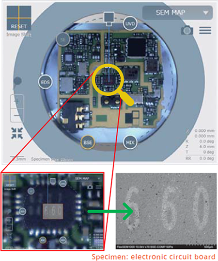
Features such as automated imaging functions and SEM MAP navigation help researchers acquire high-quality images quickly while improving workflow efficiency.
Applications Across Different Industries
Scanning Electron Microscopy supports a broad range of scientific and industrial applications, including:
- Materials Science: SEM allows researchers to examine grain structures, inclusions, fractures, corrosion, and material interfaces to better understand material performance and improve product development.
- Semiconductor Manufacturing: SEM is used to inspect wafer surfaces, microchips, solder joints, and circuit patterns, enabling manufacturers to identify defects before devices reach production.
- Industrial Quality Control: Manufacturers use SEM to verify coating quality, inspect machined components, analyze contamination, and investigate product failures to improve consistency and reduce production waste.
- Battery Research: Researchers analyze electrode materials, particle morphology, and degradation mechanisms to improve battery efficiency and lifespan.
By providing detailed surface information at the micro- and nanoscale, SEM helps laboratories make informed decisions that improve product quality, accelerate research, and support innovation.
Hitachi High-Tech Corporation. (n.d.). SEM (Scanning Electron Microscopes). https://www.hitachi-hightech.com/global/en/products/microscopes/sem-tem-stem/sem/
Hitachi High-Tech Corporation. (n.d.). Scanning Electron Microscope FlexSEM 1000 II. https://www.hitachi-hightech.com/global/en/products/microscopes/sem-tem-stem/sem/flexsem-1000-ii/
Sigmatech Inc. (n.d.). Hitachi Scanning Electron Microscope FlexSEM 1000 II. https://sigmatech.com.ph/products/hitachi-scanning-electron-microscope-flexsem-1000-ii/