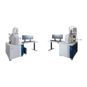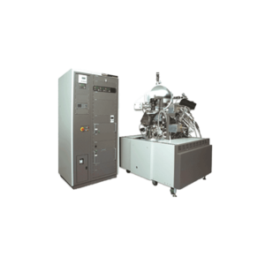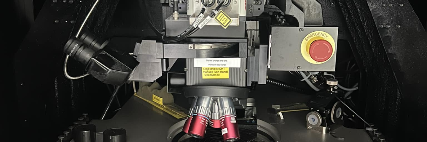

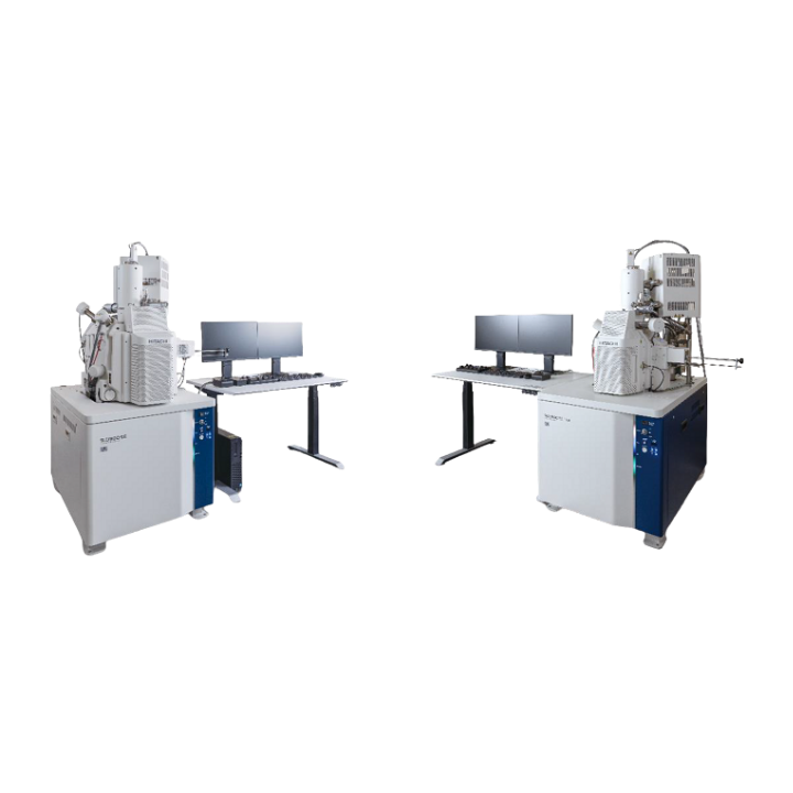
The SU3800/3900SE Series offers high-resolution FE-SEM performance combined with user-friendly, intuitive data acquisition for a wide range of applications. With the capacity to support larger and heavier specimens than most FE-SEMs on the market, the observation of substantial specimens, such as building materials, automotive, or aerospace parts, is made possible.
The SE Series lineup offers four models to expertly meet the measurement needs of a wide variety of fields: the SE Series can be configured with deceleration mode and dedicated low-energy SE detection (SE Plus models) and can be offered as both standard sample chamber and extra-large sample chamber models.
Each model provides unique capabilities; for example, the extra-large chamber models can provide the best results for foreign matter and defect analysis, helping drive quality and yield, while the Plus models are ideal for the observation of fine surface structures, creating opportunities for improvements in electronic components and semiconductor manufacturing.
All instruments from the SE series can be configured for higher throughput and automation with advanced EM Flow Creator software (option) enabling the creation and execution of customized workflows.
Schottky SEM with large specimen chamber to expand application capabilities Evaluating shapes by electron microscopy is the foundation of all material evaluation and analysis. Demand has always existed for the ability to mount and observe specimens in their original shape and condition.
The SU3900SE/SU3800SE Series Microscopes have a highly rigid multipurpose specimen chamber that makes it possible to mount specimens as is. All instruments in the SE lineup are configured with Variable-Pressure Operation as standard.
This eliminates the need to apply metal coating of non-conductive specimens and breaking or cutting large and heavy specimens, allowing observation of the sample in its original form.
SU3900SE/SE Plus
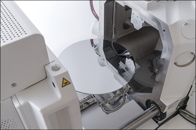
Example with 300 mm
diameter wafer loaded
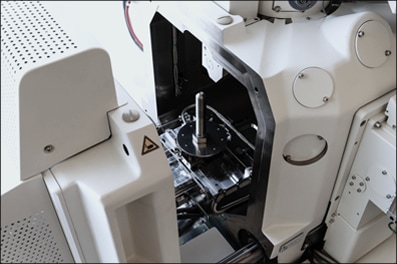
Example of a 130 mm
high metal part loaded in
the specimen chamber
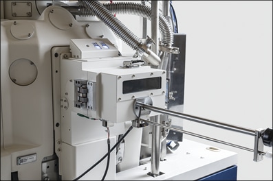
Even when using the optional specimen
exchanger, it is possible to mount
specimens with a height of up to 45 mm.
Features to facilitate specimen exchange:
Human errors can be reduced by utilizing the specimen exchange sequence, height-check gauges, touch sensors, and stage interlocks.
Explore a full walkthrough of the real specimen-exchange workflow in the video link.
Features to facilitate specimen navigation
Areas of interest can be identified by utilizing the optical camera image within the SEM MAP, up to 229 mm in diameter.
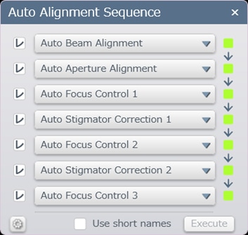
Click the video below to see a step-by-step process of specimen navigation made easy by using Hitachi’s SEM MAP technology. Auto Alignment Features Auto Alignment Sequence allows any operator, regardless of skill level, to acquire high-quality images. (Auto Alignment Sequence is a function name on software. Use as shown on the screen.)
See how easy it is to achieve high-resolution imaging by utilizing Hitachi’s Auto Alignment function by watching the video link.
High resolution for improved top-surface imaging
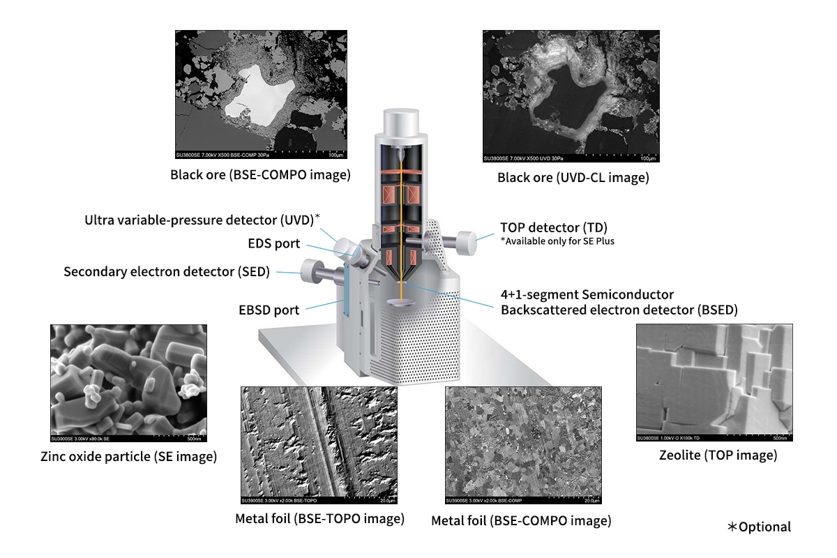
The resolution has been improved at both high and low accelerating voltages by adopting a newly developed Schottky electron gun. An advanced model (SE Plus) is also available to meet the demand for fine observation of top surface detail.
Furthermore, a high-sensitivity backscatted electron detector is included for obtaining composition and topographic information at low accelerating voltages.
This makes it possible to perform a multifaceted analysis through acquisition of a wide range of information when combined with the optional ultra-variable-pressure detector (UVD).
Automation and support functions that improve usability
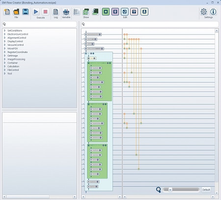
The EM Flow Creator is available to support automation of operations such as sequential image capture. A series of observation steps can be created by setting parameters, such as magnification, stage position, focus, and contrast adjustment, into blocks that can be combined, thus allowing the creation of customized recipes. Recipes can be created by dragging and dropping blocks into an arrangement like a flowchart. Automatic observation is possible by executing a created recipe.
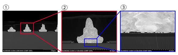
① Locate the area of interest and capture an image at x300.
② Execute the template matching function on image ① to locate a new area of interest. Then center on the location, zoom in, and capture an image at x1,000.
③ Execute the template matching function on image ② to locate a new area of interest. Then center on the location, zoom in, and capture an image at x5,000. Operator Support Functions Observation Condition Settings
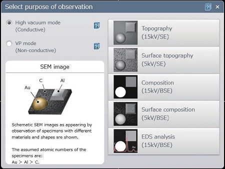
Have you ever been overwhelmed by the complexity of FE-SEM settings?
New features help ensure that observations are performed under conditions optimized for your measurement objectives.
Click the link to see how it’s done.
User Permission Settings
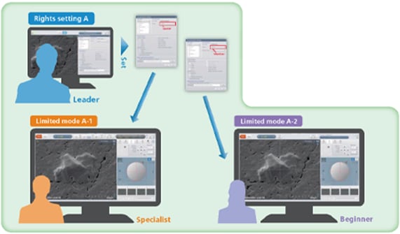
Have you ever worried about managing instruments operated by a large user base?
Administrators can define accessible functions for any type of user skill level.
Click the link to see how it’s done.
Applications Gallery
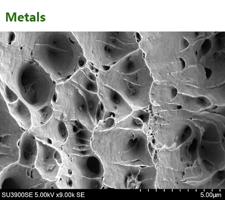
Fracture surface of iron wire
Microcavitation due to ductile failure can be seen.
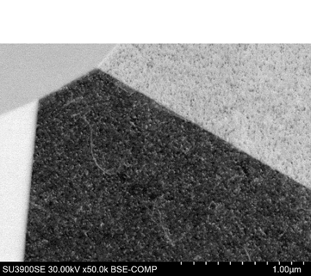
SUS316 grade austentic stainless steel
Line-like contrast suggestive of dislocations can be seen.
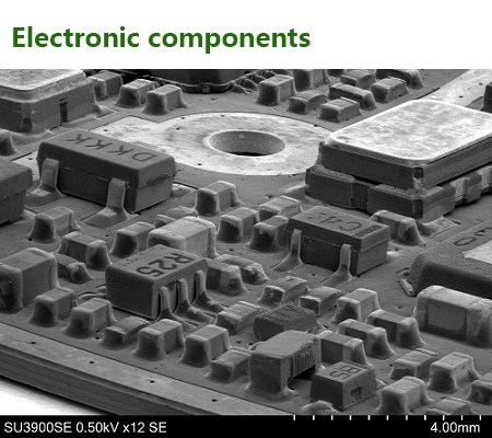
Printed circuit board
The 3D shapes and positions of mounted components can be seen using low magnification/high-tilt observation.
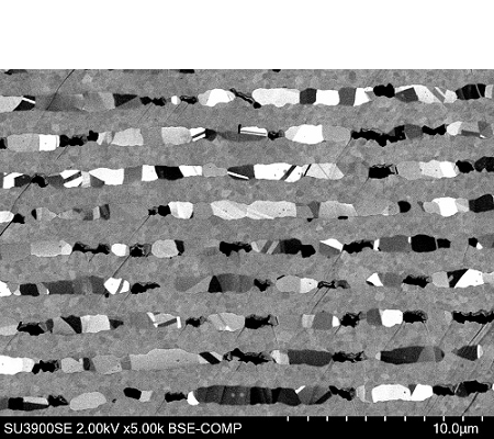
Cross section of layered ceramic capacitor
The composition and crystal contrast of nickel electrodes/dielectric layer can be observed.
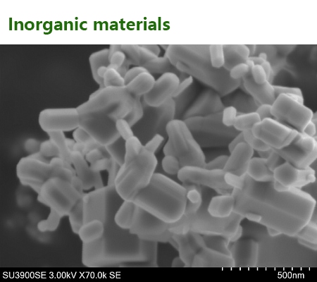
Zinc oxide particles
Fine particles with sizes of about 50 nm and 3D shape can be seen.
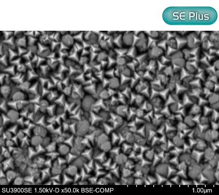
High-entropy carbide film
Distribution of particles with different compositions/shapes can be seen.
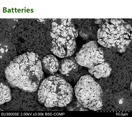
Lithium-ion battery cathode material
Distributions of cathode material particles and surrounding binder can be seen.
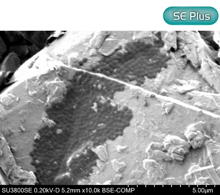
Lithium-ion battery anode material
Lithium-ion battery anode material and binder is clearly distinguished using static voltage contrast.
Specifications
| Item | SU3900SE/SE Plus | SU3800SE/SE Plus | ||
|---|---|---|---|---|
| Electron Optics | Secondary Electron Image resolution | 0.9 nm@30 kV | ||
| 2.5 nm@1 kV | ||||
| 1.6 nm@1 kV (1) (2) | ||||
| Magnification | 5~600,000× | |||
| Electron Gun | ZrO/W Schottky Emitter | |||
| Accelerating Voltage | 0.5 kV~30 kV | |||
| Landing Voltage (1) (2) | 0.1 kV~2 kV | |||
| Probe Current | Max. 150 nA | |||
| Pressure Range | Variable Pressure (VP) mode | 6 to 150 Pa | ||
| Detectors | Standard Detectors | Secondary Electron Detector (SED) | ||
| TOP detector (TD) (2) | ||||
| 41+1-segment Semiconductor Type Backscattered Electron Detector (BSED) | ||||
| Optional Detector (3) | Ultra Variable Pressure Detector (UVD) | |||
| Optional Accessories (4) | Energy dispersive X-ray detector (EDS) Electron Backscattered Diffraction Detector (EBSD) | |||
| Specimen Stage | Stage Control | 5-axis Motor Drive | ||
| Movable Range | ||||
| X | 0~150 mm | 0~100 mm | ||
| Y | 0~150 mm | 0~50 mm | ||
| Z | 3~85 mm | 3~65 mm | ||
| T | -20~90° | |||
| R | 360° | |||
| Specimen Chamber | Mountable Specimen Size | Max. φ 300 mm Height: 130 mm | Max. φ 200 mm Height: 80 mm | |