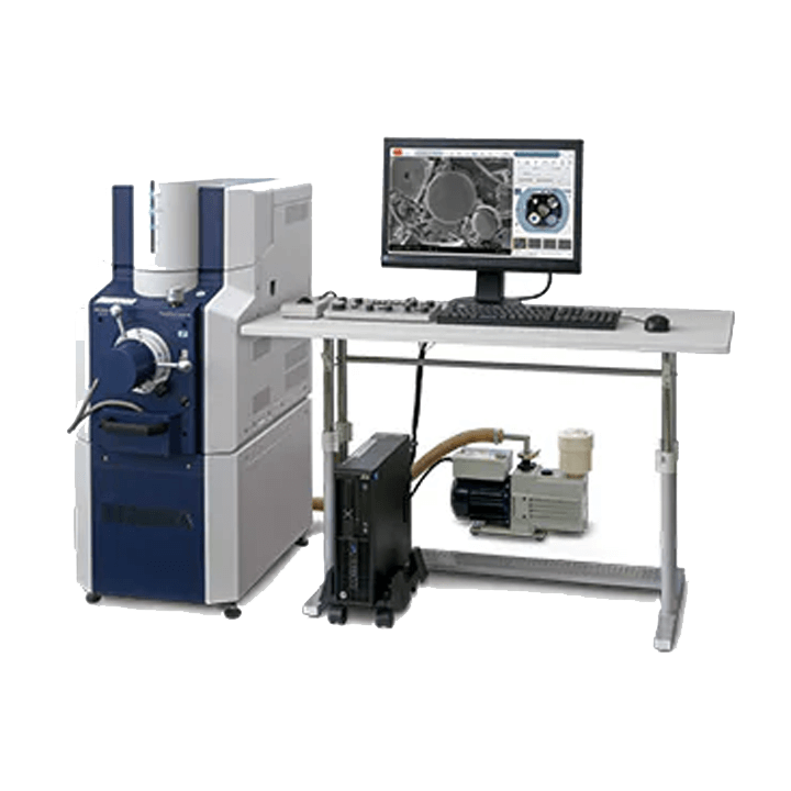
The FlexSEM 1000 II VP-SEM combines innovative technological features with an intuitive interface, to deliver adaptability and flexibility in a powerful, automated, lab-friendly package. Cutting-edge technology and circuitry provides unrivaled imaging performance, even in variable-pressure environments, a feature previously only available in a full-sized SEM. This SEM runs on clean energy for an economical analytical tool, without compromising performance.

Features

The FlexSEM 1000 II Scanning Electron Microscope features newly designed electron optical and signal detection systems providing unparalleled imaging and analytical performance in a lab-friendly configuration. Keeping efficiency in mind, the FlexSEM features an adaptable, separable, and compact design, such that it can be installed in limited office, laboratory, or even mobile spaces. Engineered to appeal to both the novice and expert microscopist for a wide range of applications, including biological and advanced material specimens, this microscope will certainly expand your analyses as well as your expectations.

Compact & High-Performance Column

Best-in-class resolution in a compact system. The FlexSEM employs a newly designed electrical optical system with a reliability-proven high-sensitivity detector, achieving imaging at 4 nm.

High resolution image

The electron optics incorporate a low aberration objective lens and a unique gun bias system that allows delivery of high emission current.
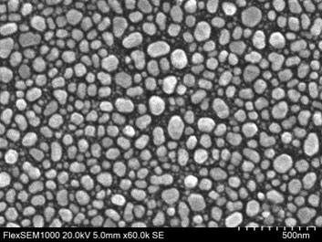
Secondary Electron (SE) Image
Accelerating Voltage: 20 kV
Secondary Electron (SE) Image
Magnification: 60,000X
Resolution: 4.0 nm
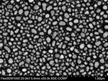
Backscattered Electron (BSE) Image
Accelerating Voltage: 20 kV
Backscattered Electron (BSE) Image
Magnification: 50,000X
Resolution: 5.0 nm

Ultra-Variable-Pressure Detector

Novel low vacuum technologies enable observation of the surface of non-conductive specimens without preprocessing, across the entire pressure and accelerating voltage ranges.

New & Improved Auto Functions

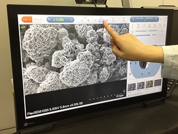
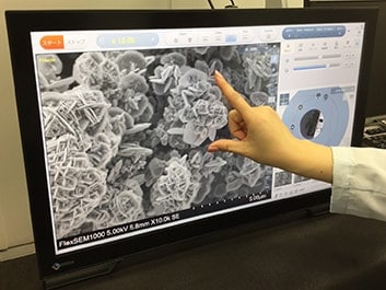
The user interface is easy to operate even by novice users, and with the various automated functions, high-quality and quick data acquisition can be accomplished regardless of user experience level. A touch panel operation is possible.
-
-

Intuitive & Correlative Navigation

SEM MAP helps to locate regions of interest quickly, and delivers accurate correlated optical and SEM images using only one click. Optical and EM correlation function, SEM MAP is fully integrated into the graphical user interface.

COMPACT SLIM BODY

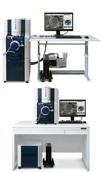
A compact design (450 mm wide) minimizes system footprint. The FlexSEM is designed with separable units for flexible system placement. The entire system requires only a standard wall outlet for power.
-
FlexSEM 1000 II

UNPARALLELED IMAGE QUALITY

The newly developed electron optical column and Ultra-Variable-Pressure Detector (UVD) enable superior imaging of specimen surfaces at low-accelerating-voltages and low-vacuum conditions.
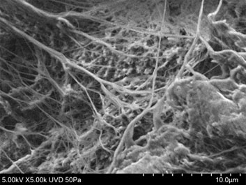
Functional Resin Fracture
Sample: Functional Resin Fracture
Vacc: 5 kV; Mag: 5,000X
Pressure: 50 Pa; Signal: UVD
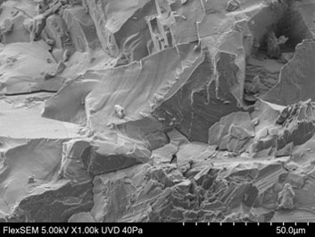
Pyrite Fracture Surface
Sample: Pyrite Fracture Surface
Vacc: 5 kV; Mag: 1,000X
Pressure: 40 Pa; Signal: UVD

INTUITIVE OPERATION

The user-friendly GUI as well as accurate and fast Auto Focus Control (AFC) and Auto Brightness and Contrast Control (ABCC) algorithms, take only 5 seconds to enable optimized imaging performance with minimal time and effort.

NEW CAMERA NAVIGATION – “SEM MAP”

The “SEM MAP” function makes traversing across an entire specimen effortless. Navigate your sample with the use of an optical camera, and deliver accurate correlated Optical and SEM images using only one click.

Applications


Materials Science

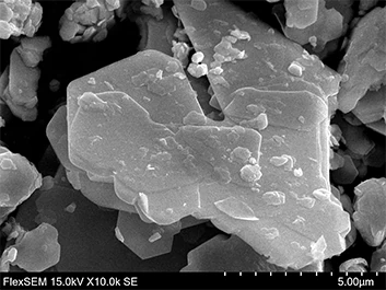
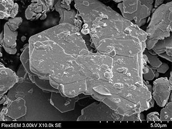
Tungsten disulfide

Accelerating Voltage: 15 kV
(a) Accelerating Voltage: 15 kV
Accelerating Voltage: 3 kV
(a) Accelerating Voltage: 3 kV

Magnification: 10,000X
Signal: SE, Without metal coating

Point of View
The FlexSEM employs an Opti-Bias system that provides higher emission current at low kV for optimum brightness. The result is best-in-class image sharpness (S/N) at a low accelerating voltages.

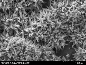
Hydrogen absorbing alloy

Accelerating Voltage: 15 kV
Accelerating Voltage: 5 kV
Magnification: 30,000X
Signal: SE, Without metal coating

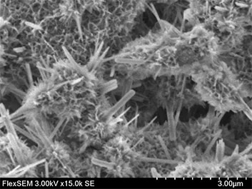
Cement

Accelerating Voltage: 3 kV
Magnification: 15,000X
Signal: SE, Without metal coating

Biology

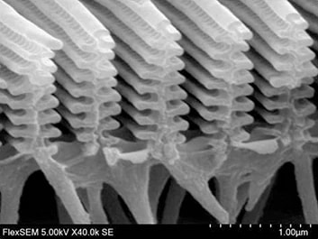
Butterfly wing

Accelerating Voltage: 15 kV
Accelerating Voltage: 5 kV
Magnification: 40,000X
Signal: SE, With metal coating

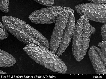
Pollen

Accelerating Voltage: 3 kV
Accelerating Voltage: 5 kV
Magnification: 500X
Signal: UVD, Without metal coating

Semiconductors

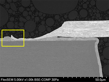
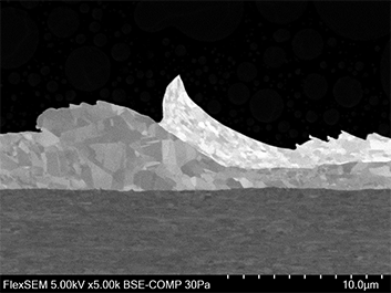
Wedge Bond

Accelerating Voltage: 15 kV
Accelerating Voltage: 5 kV
Vacuum: 30 Pa
Magnification: 1,000X
Signal: BSE, Without metal coating
Accelerating Voltage: 3 kV
Accelerating Voltage: 5 kV
Vacuum: 30 Pa
Magnification: 5,000X
Signal: BSE, Without metal coating


Related Products

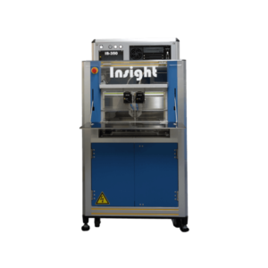
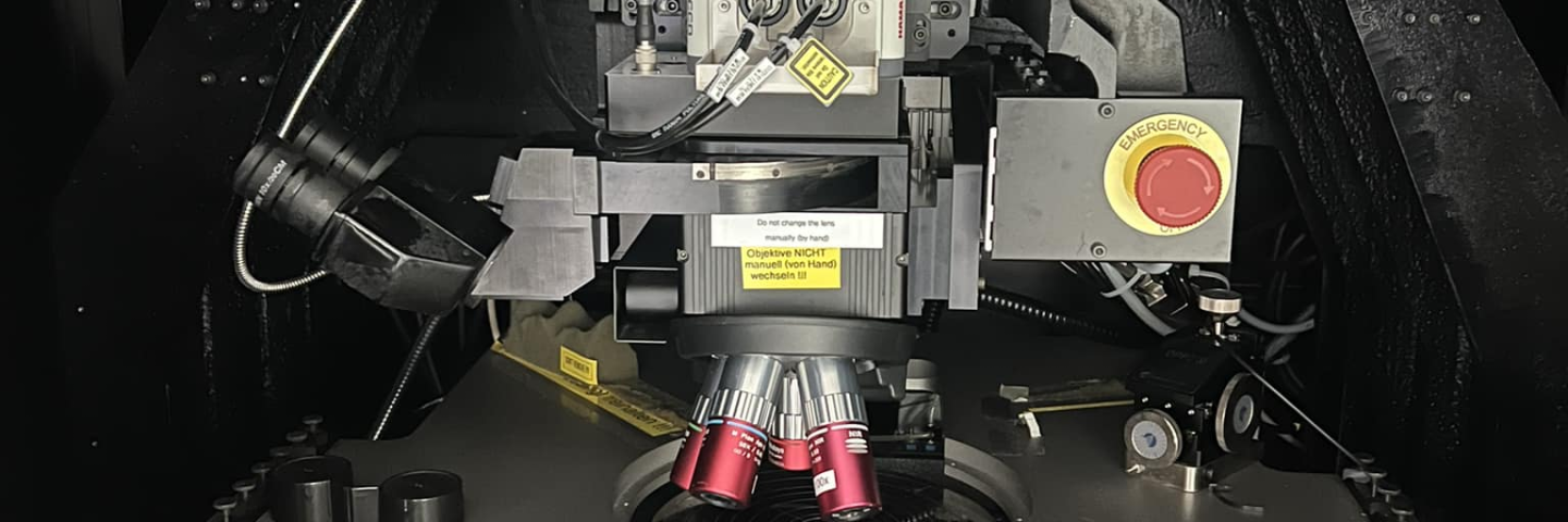
IR-2200 Microscope System enables the user to inspect sub-surface images including MEMS device, 3D stacks, incoming wafers, photovoltaic and wafer level CSP’s with an astonishing level of precision.
Ultraslice Macrotome is a low-cost sectioning system designed for mobile chips, devices, and various industrial samples. This system is known for its precision and versatility.
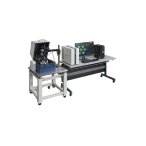
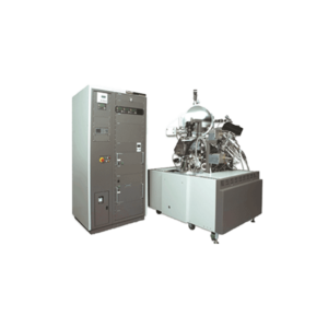
Ethos offers powerful solutions integrated into a single platform including low-acceleration Ar/Xe ion-beam processing when configured as a Triple-Beam system.
Solution for the review of defects of semiconductor integrated circuit detected by AOI/AVI at front end processing, helps to eliminate false defects and increase overall yield.
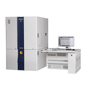
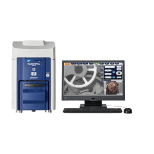
The FlexSEM 1000 II VP-SEM combines innovative technological features with an intuitive interface, to deliver adaptability and flexibility in a powerful, automated, lab-friendly package.
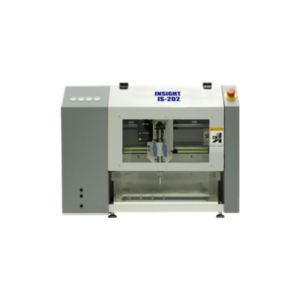
The Insight-Scan (IS) series of Scanning Acoustic Microscopes(SAM) integrates the finest state-of-the-art technology for high resolution, high speed, fully digital non-destructive sample analysis.
The MC1000 Ion Sputter Coater is a sample preparation instrument for use with a Scanning Electron Microscope (SEM) designed to deposit a thin metal coating, such as platinum (Pt), gold (Au), platinum-
The IM4000Plus Ion Milling System utilizes a broad, low-energy Ar+ ion beam milling method to produce wider, undistorted cross-section milling or flat milling.
The K850 combines versatility and ease of operation. Built-in thermo-electric heating and adiabatic cooling allow precise temperature control.
PHI’s Latest Generation of TOF-SIMS, having a Modern Ergonomic Package, Smaller Footprint, and Advanced Features

How can we help?

You may contact our specialists by accomplishing form below.

Website menu

Download catalog

To download e-catalog, please submit your details below.

Hamamatsu Failure Analysis

Subscribe to newsletter

Sign up for our newsletter to get updates on promos, seminars, events, products, application notes and more.

Inquire About this Product

You may contact our specialists by accomplishing form below.

Scanning Electron Microscope
FlexSEM 1000 II
Scanning Electron Microscope
FlexSEM 1000 II