What is Scanning Electron Microscopy (SEM)?

In the realm of microscopy, Scanning Electron Microscopes (SEM) stand out as a powerful tool for detailed imaging and analysis. Whether you’re in materials science, biology, or industrial research, understanding how SEMs work and their applications can be incredibly beneficial.

What is a Scanning Electron Microscope (SEM)?

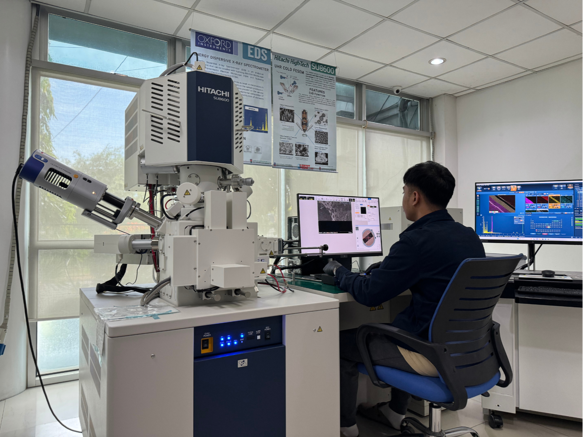
A Scanning Electron Microscope (SEM) is a type of electron microscope that produces high-resolution images of a sample by scanning its surface with a focused beam of electrons. Unlike traditional light microscopes, SEMs use electrons instead of light to form an image, allowing for much higher magnification and resolution.

How Does a Scanning Electron Microscope Work?

The working principle of an SEM involves several key steps:

  1. Electron Beam Generation: An electron gun generates a beam of electrons.
  2. Beam Focusing: Electromagnetic lenses focus the electron beam onto the sample.
  3. Scanning: The focused beam scans the sample in a raster pattern.
  4. Interaction and Signal Detection: As the electrons interact with the atoms in the sample, various signals are produced, including secondary electrons, backscattered electrons, and characteristic X-rays.
  5. Image Formation: Detectors collect these signals and convert them into an image, revealing detailed information about the sample’s surface topography and composition

Typical types of Scanning Electron Microscopes

There are various types of SEMs designed to meet different needs:

  • Tabletop SEMs: Compact and user-friendly, ideal for educational purposes and small-scale research.
  • Benchtop SEMs: Slightly larger than tabletop models, offering higher resolution and more advanced features.
  • Floor Model SEMs: Large, high-performance instruments used in advanced research and industrial applications
  • Environmental SEMs (ESEM): Capable of imaging wet or non-conductive samples without extensive preparation

Attachments and Enhancements

SEMs can be equipped with various attachments to enhance their capabilities including:

  • Energy Dispersive X-ray Spectroscopy (EDX): Allows for elemental analysis by detecting characteristic X-rays emitted from the sample.
  • Electron Backscatter Diffraction (EBSD): Provides crystallographic information by analyzing backscattered electrons.
  • Cathodoluminescence (CL): Used to study optical properties by detecting photons emitted from the sample

Related Instrumentation

The FlexSEM 1000 II VP-SEM combines innovative technological features with an intuitive interface, to deliver adaptability and flexibility in a powerful, automated, lab-friendly package.
The SU7000 is the ultimate high-performance all-rounder: an ultra high resolution Schottky FESEM offering nanoscale imaging and powerful analysis
The Cold Field Emission source is ideal for high-resolution imaging with a small source size and energy spread. Innovative CFE Gun technology contributes the ultimate FE-SEM with superior beam bright
The SU8600 incorporates a highbrightness cold-field emitter (CFE) to allow acquisition of ultra-high-resolution images even at low accelerating voltages.
Ethos offers powerful solutions integrated into a single platform including low-acceleration Ar/Xe ion-beam processing when configured as a Triple-Beam system.
Hitachi High-Tech’s scanning electron microscopes SU3800/SU3900 deliver both operability and expandability. The operator can automate many operations and efficiently utilize their high performance.
This new generation of the long-standing Hitachi tabletop microscopes (TM) integrates ease of use, optimized imaging, and high-image quality, while maintaining compact design

Need assistance?

Our experts are here to help.

Product added to Quote list ✔

failure analysis, material characterization, and metrology equipment

Subscribe to newsletter

Sign up for our newsletter to get updates on promos, seminars, events, products, application notes and more.