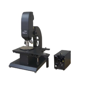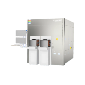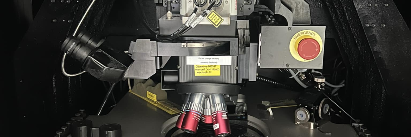
The semiconductor industry continues to push the limits of miniaturization, enabling smaller, faster, and more powerful electronic devices. As integrated circuits become increasingly complex, manufacturers must detect and evaluate microscopic defects before they affect device performance or reduce production yield.
Automated Optical Inspection (AOI) systems have become an important part of semiconductor production by identifying potential defects during wafer fabrication. However, detecting a defect is only the first step. Engineers must still verify whether the detected feature is a true defect, determine its severity, and identify its possible root cause.
Manual review of thousands of inspection results can be time-consuming and inconsistent. Automated wafer defect review systems address this challenge by rapidly locating detected defects, capturing high-resolution images, and organizing inspection data for efficient analysis. These systems help semiconductor manufacturers reduce inspection time, improve defect classification, and accelerate process improvements throughout wafer production.
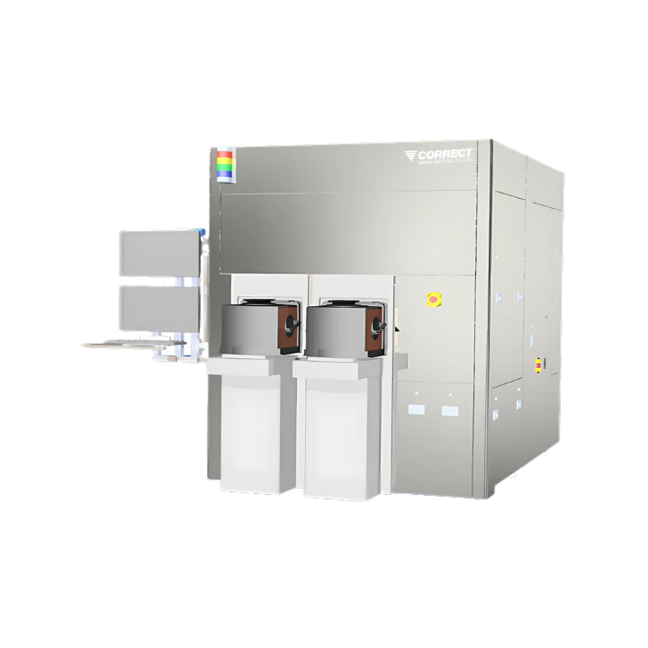
The Seiwa Optical Semiconductor Auto Review System automates wafer defect review by providing high-speed optical inspection and accurate defect verification.
What Is Automated Wafer Defect Review?
Wafer defect review is the process of examining defects previously detected by Automated Optical Inspection systems. Instead of rescanning the entire wafer, review systems navigate directly to reported defect locations and capture detailed images for further evaluation.
This process enables engineers to:
- Verify AOI inspection results
- Classify defects accurately
- Distinguish real defects from false detections
- Monitor manufacturing trends
- Improve process control
- Increase production yield
Automated review significantly reduces inspection time while providing consistent imaging and documentation for semiconductor manufacturing.
How the Seiwa Optical Semiconductor Auto Review System Improves Inspection
The Seiwa Optical Semiconductor Auto Review System is designed to automate the review of defects identified during wafer inspection. By importing coordinate data from Automated Optical Inspection systems, the instrument automatically moves to each defect location and captures detailed optical images for verification.
Its On-Fly measurement capability enables rapid inspection while maintaining high positioning accuracy, allowing engineers to review large numbers of defects in less time than conventional manual methods.
The system is capable of identifying pattern defects, contamination, scratches, cracks, and other wafer surface abnormalities. By combining automated navigation with high-resolution imaging, it supports efficient defect analysis and helps manufacturers optimize production processes.