
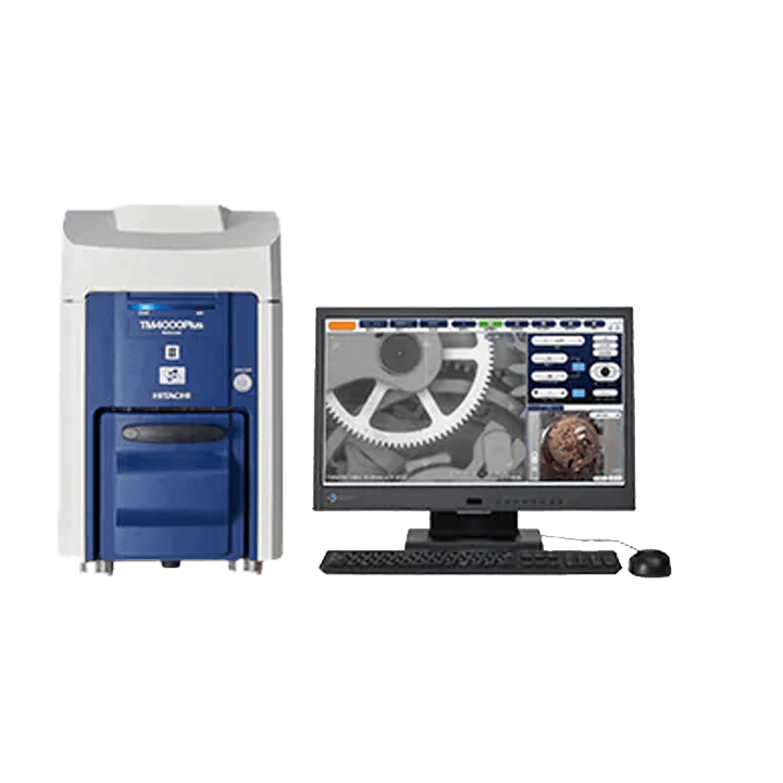
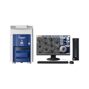
Tabletop Scanning Electron Microscope Philippines
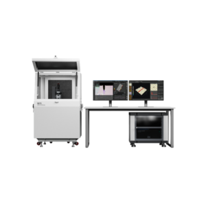
The Hitachi TM4000II and TM4000Plus II Scanning Electron Microscopes (SEM) offer advanced imaging capabilities with user-friendly operation. These tabletop SEMs provide high-resolution images and elemental analysis, making them ideal for research, quality control, and educational applications. Available in the Philippines through Sigmatech Inc.
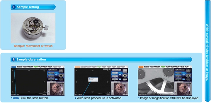
A quality image can be obtained with simple steps.
Automation, Observation, and Elemental Analysis
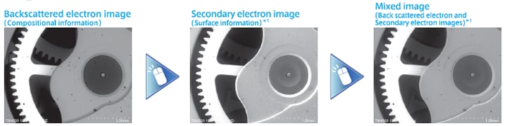
Easy to switch images with one-click.
Rapid acquisition of elemental maps *2

Sample : Movement of watch
*1Secondary electron images and MIX images can only be observed in TM4000Plus II
*2Option
Intuitive operation on Camera Navi *
Use of optical images helps navigate to target observation area easily.
Obtained SEM images can be layered on a SEM MAP image.
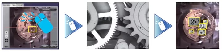
Sample: Movement of watch
*Option: Camera Navigation System
Report Creator
Simply select images and a template to create a customized reports.
Created reports can be saved/edited in Microsoft Office® formats.
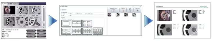
Sample : Movement of watch
The image on the screen includes options.
Various imaging applications using 4-under low vacuum status.
Charge-up reduction mode
Charge on a sample can be reduced by one-click.
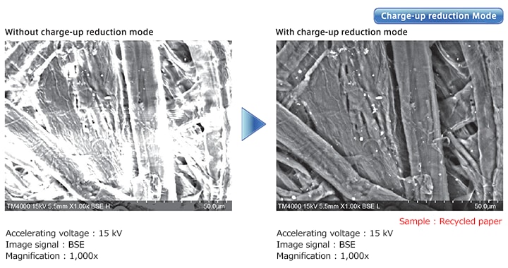
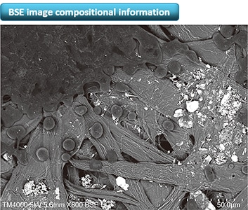
Image a variety of materials under low vacuum condition
The images show observations of non-conductive samples such as ink toner particles and a hydrated leaf surface.
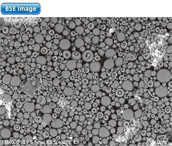
Accelerating voltage: 5 kV
Image signal: BSE
Magnification: 2,500x
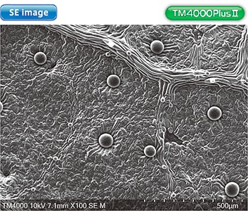
Accelerating voltage: 10 kV
Image signal: SE
Magnification: 100x
Various imaging applications using 4-under low vacuum status.
Innovative secondary-election detector to obtain surface detail with non-conductive samples at lower vacuum conditions
The TM4000Plus II can observe not only conductive samples, but also non-conductive or hydrated samples without sample preparation. Switching between BSE and SE can be performed easily.
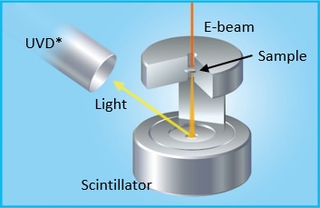
High-sensitivity Low vacuum SE Detector (UVD)
Hitachi’s UVD generates secondary-electron images by detecting visible light excited by electron gas interactions.
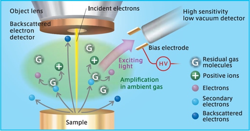
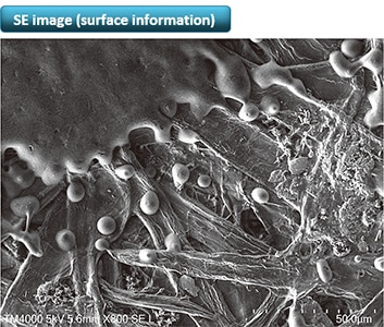
Image signal: SE
Magnification: 800x
Accelerating voltage: 5 kV
Image signal: BSE
Magnification: 800x
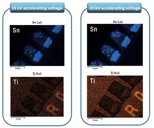
Advantages of 20 kV accelerating voltage
High accelerating voltage enables higher-speed EDS analysis.
EDS mapping data at 20 kV in 2 min
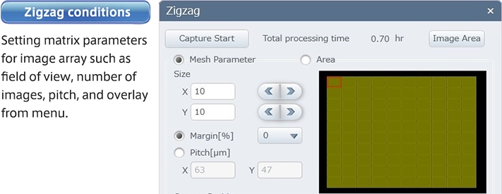
Multi Zigzag (Option)
A function that takes multiple high-magnification images and stitches them together to create a single high-resolution image.
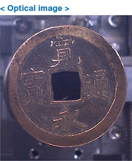
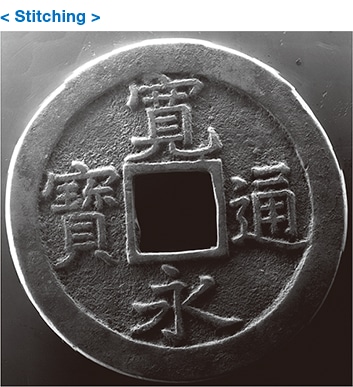
Accelerating voltage: 15 kV
Image signal: SE
Magnification: 30x
Field of view 10 vertically × 12
horizontally
(some parts were trimmed)
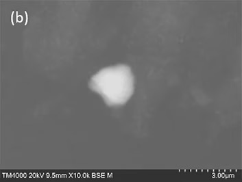
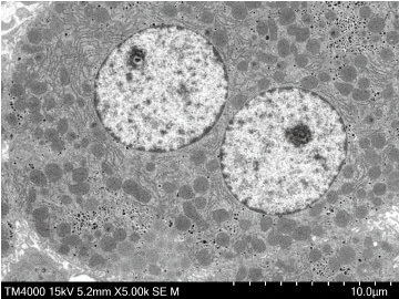
STEM holder (Option)
Easily obtain transmitted images on thin samples
The newly developed STEM holder can be used to perform transmission images with the Hitachi UVD. Images of thin or biological samples can be obtained.
*UVD is a function of TM4000Plus II.
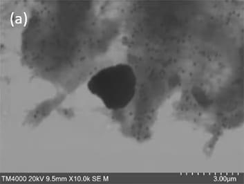
Accelerating voltage : 20 kV
Image signal : (a) STEM, (b) BSE
Magnification : 10,000 x
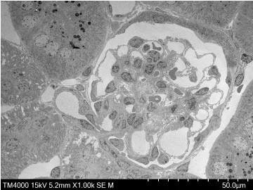
Accelerating voltage : 15 kV
Image signal : STEM
Magnification : 1,000 x
Accelerating voltage : 15 kV
Image signal : STEM
Magnification : 5,000 x Specifications Model name TM4000Plus II TM4000 II Magnifications 10× – 100,000× (Photographic magnification)
25× – 250,000× (monitor display magnification) Accelerating voltage 5 kV, 10 kV, 15 kV, 20 kV Image signal Backscattered electron
Secondary electron
Mix (Backscattered electron + Secondary electron) Backscattered electron Vacuum mode BSE: Conductor/Standard/Charge-up reduction
SE: Standard/Charge-up reduction
Mix: Standard/Charge-up reduction BSE: Standard/Charge-up reduction Sample stage traverse X: 40 mm, Y: 35 mm Maximum sample size 80 mm (diameter), 50 mm (thickness) Electron gun Pre-centered cartridge tungsten filament Signal detection system High-Sensitivity 4-segment BSE detector
High-Sensitivity Low-Vacuum SE detector (UVD) High-Sensitivity 4-segment BSE detector Evacuation system
(vacuum pump) Turbo molecular pump : 67 L/s×1 unit
Diaphragm pump : 20 L/min×1 unit Size / weight Main unit (motorized stage): 330 (width)×614 (depth)×547 (height) mm, 54 kg
Main unit (manual stage): 330(width)×617(depth)×547(height) mm, 54 kg
Diaphragm pump: 144 (width)×270 (depth)×216 (height) mm, 5.5kg


")
")
