Seiwa Wafer review system visually inspects the defect location detected from AOI systems. By importing the inspection system data results from the AOL, this review system is able to capture the visual data and add it to previous inspection results.

Key Industries: Semiconductor and Electronics and more.

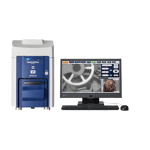
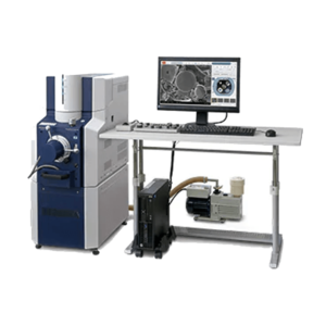
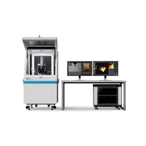
Seiwa Wafer inspection system visually inspects the defect location detected from AOI systems. By importing the inspection system data results from the AOL, this review system is able to capture the visual data and add it to previous inspection results.

Brochure >

Features

Related Products

Ultraslice Macrotome is a low-cost sectioning system designed for mobile chips, devices, and various industrial samples. This system is known for its precision and versatility.
The top of the line ion-milling system for producing exceptional quality cross section or flat-milling samples for electron microscopy.
The HT7800 RuliTEM is a 120 kV transmission electron microscope (TEM) with multiple lens configurations, including a standard lens for unsurpassed high contrast and a class-leading HR lens.
Solution for the review of defects of semiconductor integrated circuit detected by AOI/AVI at front end processing, helps to eliminate false defects and increase overall yield.
The K850 combines versatility and ease of operation. Built-in thermo-electric heating and adiabatic cooling allow precise temperature control.
The ZONESEMⅡ Tabletop Sample Cleaner uses UV-based cleaning technology to minimize or eliminate hydrocarbon contamination for electron microscopy imaging.
DSC is used to measure heat flow for material characterization by providing thermal properties such as melting point, glass transition and crystallization.
The PHEMOS-X is a high-resolution emission microscope that pinpoints failure locations in semiconductor devices by detecting the weak light emissions and heat emissions caused by defects.
ULTRAPOL Advance has been designed to be an all-in-one lapping & polishing workstation for the production of flat surfaces.
The AFM100 Series is Hitachi’s next generation probe microscopy platform.

How can we help?

You may contact our specialists by accomplishing form below.

failure analysis, material characterization, and metrology equipment

Subscribe to newsletter

Sign up for our newsletter to get updates on promos, seminars, events, products, application notes and more.

Inquire for this Product

Wafer Inspection System