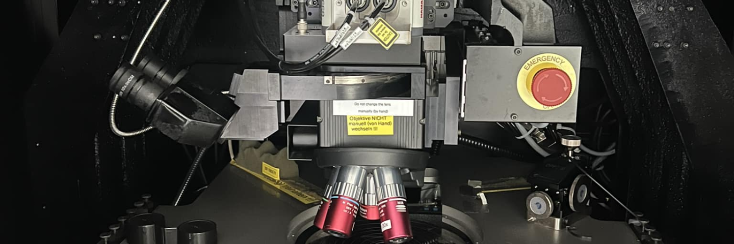
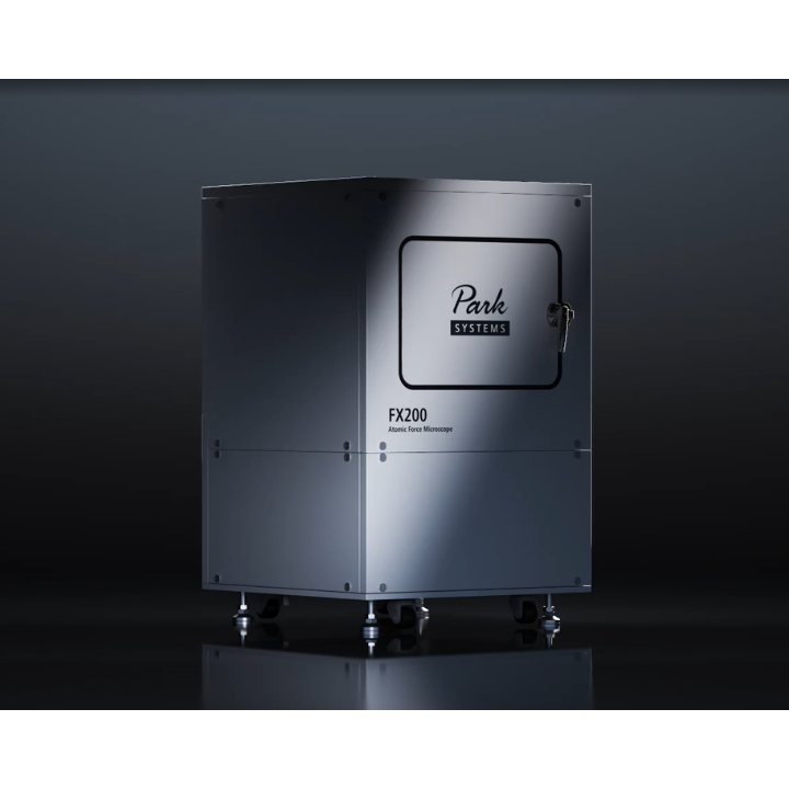
As electronic devices become smaller and materials become more advanced, researchers need analytical tools capable of measuring surface features at the nanometer scale without compromising accuracy. Whether developing semiconductor wafers, advanced coatings, battery materials, or precision-engineered components, understanding surface topography is essential for improving product quality and accelerating innovation.
Atomic Force Microscopy (AFM) has become one of the most trusted techniques for nanoscale surface characterization because it provides three-dimensional surface measurements with exceptional vertical resolution. Unlike conventional optical microscopes, AFMs capture surface details that are impossible to observe using visible light alone.
Modern laboratories also face another challenge: analyzing increasingly larger samples while maintaining high measurement precision. This demand has led to the development of large-sample AFMs such as the Park FX200, which combines advanced automation with high-resolution imaging to support research and industrial metrology.
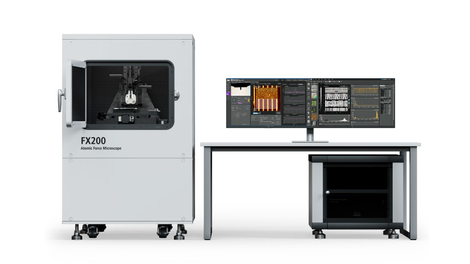
The Park FX200 Large Sample AFM provides high-resolution nanoscale imaging with automated workflows for research and industrial metrology.
Why Large-Sample AFMs Are Becoming More Important
Many modern applications involve samples much larger than traditional AFM systems were originally designed to accommodate. Semiconductor wafers, advanced electronic packages, optical components, and engineered materials often require measurements across larger surfaces while still maintaining nanometer-scale precision.
Large-sample AFMs allow researchers to inspect multiple areas on a single specimen without repeatedly repositioning the sample. This improves workflow efficiency, enhances measurement repeatability, and reduces the time required for comprehensive surface analysis.
The Park FX200 accommodates samples up to 200 mm, allowing researchers to inspect larger specimens with precise positioning and repeatable measurements.
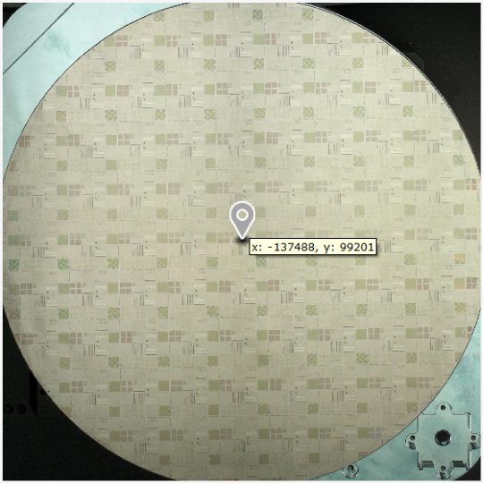
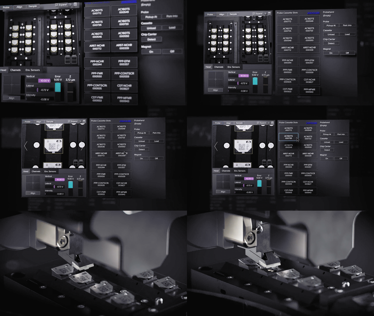
Automated probe exchange and intelligent workflow features help improve efficiency while maintaining consistent nanoscale measurements.
Applications Across Different Industries
The Park FX200 supports a wide range of scientific and industrial applications, including:
- Semiconductor wafer inspection
- Advanced materials research
- Thin-film characterization
- Nanotechnology research
- Battery materials development
- Surface roughness measurement
- Failure analysis
- Research and development laboratories
Its combination of large-sample capacity, automated operation, and high-resolution imaging makes it a versatile platform for organizations that require precise surface metrology across multiple disciplines.
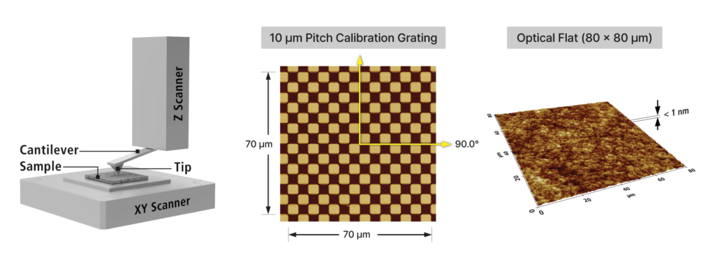
Park Systems’ proprietary scanning technology enables highly accurate surface measurements while minimizing imaging artifacts and protecting delicate samples.
As industries continue to develop smaller devices and more sophisticated materials, the demand for accurate nanoscale surface analysis continues to grow. Large-sample atomic force microscopes provide researchers with the ability to analyze complex surfaces efficiently while maintaining exceptional measurement precision.
The Park FX200 combines large-sample capability, advanced automation, and proprietary AFM technologies into a single platform, helping laboratories improve productivity while delivering reliable nanoscale measurements for research, quality control, and advanced manufacturing.
Park Systems. (n.d.). Park FX200 large sample AFM. https://www.parksystems.com/en/products/research-afm/large-sample-afm/fx200
Sigmatech Inc. (2026). Park FX200 large sample AFM. https://sigmatech.com.ph/products/park-fx200-large-sample-afm/