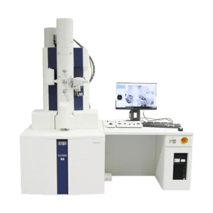
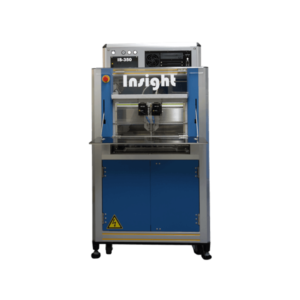
Hitachi Ethos FIB-SEM Features
Key Features
1. High-Performance FE-SEM Column with Dual Lens Mode
- Ultra-high-resolution observation (HR mode: semi-in-lens)
- High-accuracy end-point detection in real time (FF mode: Field Free (time sharing mode))
2. High-Throughput Material Processing
- Ultra-fast processing with high ion-current density (Max. beam current: 100 nA)
- User programmable script for auto processing and observation
3. Microsampling System
- Fully integrated sample-orientation control for Anti-Curtaining Effect (ACE technology)
- TEM sample preparation for uniform lamellas at any orientation
4. Triple-Beam Capable, Delivering Advanced Quality Results
- Low-acceleration noble-gas ion-beam material processing
- Innovative functions reduce Ga ion related and other milling artifacts
5. Large Multi-Port Chamber and Stage for Various Applications
- Large sample size capable system with exceptional stage stability
- Full range enhanced long-distance tracking (155 x 155mm)
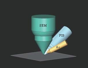
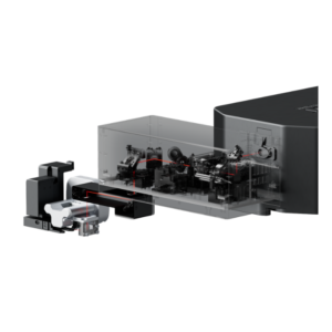
Refined Electron Optics and Multi-Signal Detection
The Ethos SEM column is composed of a magnetic- and electrostatic-field compound objective lens system configured as two lens modes. High Resolution (HR) mode achieves sample observation at ultimate resolution by immersing the sample within the magnetic field of the lens system. Field Free(FF) mode offers real-time FIB processing for high accuracy end point milling. Hyper switching between FIB irradiation and SEM imaging as fast as 10 nsec offers real-time fabrication and observation views with clarity. Fast SEM and IM imaging enables users to quickly find the area of interest with ease.
High-Resolution SEM Imaging
High-Performance FIB
High-current-density FIB for high-speed and large-area processing.
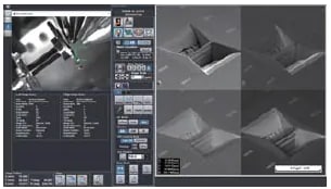
Auto-pilot software supports a multitude of automated functions for imaging, TEM lamella preparation, cross-section generation, and more…
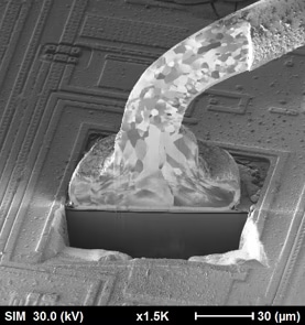
High speed ion milling, SIM image
highlighting grain contrast of bond wire
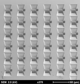
Multiple sites processed for lift out by
Auto-pilot Automation software
Time Sharing Mode
Time sharing mode is the ultimate tool to maximize SEM observation while ion milling simultaneously.
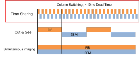
Features:
■ Time Sharing mode resolves high-quality SEM imaging with any detector and any milling condition for end-point detection in real time.
■ Cut & See mode for ultra-high resolution imaging in HR mode.
■ Simultaneous observation for traditional imaging
Cut & See for 3D structural analysis
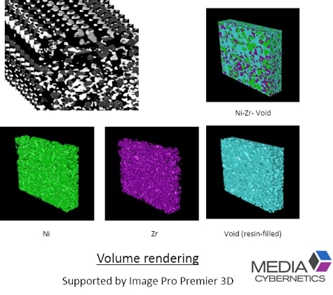
FOV: 20 μm
Number of cut: 200
Cutting interval: 20 nm
SEM accelerating voltage: 1.5 kV
Sample: Fuel cell electrode (Ni-YSZ)
Sample courtesy of Prof. Naoki Shikazono,
Institute of Industrial Science,
The University of Tokyo
High-Quality TEM Specimen Preparation Using Triple-Beam Technology
Ethos offers powerful solutions integrated into a single platform including low-acceleration Ar/Xe ion beam processing when configured as a Triple-Beam system.
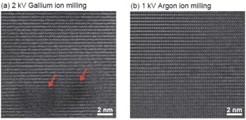
Dark contrast (red arrow) areas indicates Gallium ion induced damage at 2 kV.
The right image shows the same single-crystal structure intact after applying 1 kV Argon ion milling revealing clear crystal lattice fringes.
Triple-Beam System (Argon / Xenon)
Low-energy Ar/Xe broad ion milling mitigates amorphous material resulting from gallium ion milling.
ACE: Anti Curtaining Effect
Optimized GUI for Maximum Efficiency
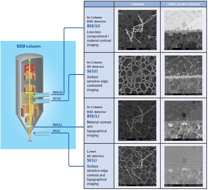
Enhanced signal selectivity with 4 detectors
■ Four-channel simultaneous signal acquisition of In-Column detectors (SED x 1, BSE x 2) and In-Chamber SE detector
■ Programmable menus to save and recall SEM and FIB beam parameters
■ Selective and discreet imaging from various detectors enabling specific user applications such as compositional or topographical imaging
■ Condition saving and recalling are possible for each signal mode such as gain levels, contrast, and brightness in addition to other parameters
Next-Generation Interface for Custom Processing Modes and Recipes
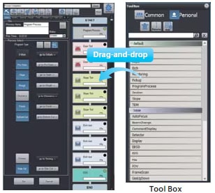
Graphically driven programming for macro visualization
■ Simple drag-and-drop interface to create complex processing/observation recipes with ease
■ Fully programmable processing modes with nested templates
■ Maximum efficiency for routine operation by utilizing registered recipes
Superior flexibility for creating your recipe
■ Multifaceted processing modes including slope and bitmap processing as well as preset patterns including rectangles, circles, and trapezoids
■ Predefined recipes for cross-section processing and TEM lamella preparation
■ Vector scan software allows custom processing applications
■ High-accuracy and automated processing with drift correction
■ Recipes can be individual or group-based for multi-user lab environments.
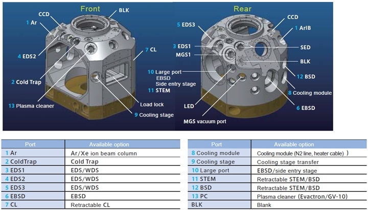
Sample Chamber and Stage for Various Applications
■ Newly designed sample stage for high resolution imaging
■ A variety of analytical configurations are possible with optimum detector positioning.

For more information, contact us.


")
")