The IS-350 Scanning Acoustic Microscope is the versatile workhorse in the InsightScan family of acoustic microscopes. Its large sample holder and scan area, high spatial resolution, fast acquisition speed and large bandwidth make it a powerful lab instrument for high resolution R&D applications and at the same time a perfectly suitable instrument for high volume quality control in production environment.

Key Industries: Aerospace, Automotive, Semiconductor and Electronics and more.

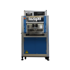
Powerful scan technology

  • High speed technology: 1000 mm/sec scan speed, 500 MHz receiver bandwidth, 3 GHz data sampling rate
  • Dual channel data acquisition for minimizing the acquisition time on one sample, or for simultaneous data acquisition on 2 different samples
  • Simultaneous pulse-echo and through transmission acquisition supported
  • Up to 6 axis control, including 2-fold transducer tilt for wedge and contour scans

Advanced software features

  • Real time full waveform acquisition: Collected data allow offline rescanning of the sample with different gate settings
  • Advanced analysis features: Generation of virtual B-scans and tomographic C-scans from stored data files
  • Slice scan for acquisition of a virtually unlimited number of C-scans on different depth levels simultaneously
  • Multi-lingual software in English, Japanese, Chinese, French, German, …

 Wide application range

      Semiconductor and microelectronics

  • CSP and Flip Chip underfil void evaluation and delamination analysis
  • Power semiconductor integrity evaluation
  • Internal defect inspection: Inclusions, cracks, die tilt
  • Interface evaluation of bonded wafers

      Material analysis

  • Inclusion, crack and void detection in metals, plastics, resin

      Interface analysis

  • Void evaluation in welds and brazed interfaces
  • Electrostatic chuck void detection
  • Delamination of composite materials
  • Interface analysis on heterogeneous assembled materials

Related Products

Solution for the review of defects of semiconductor integrated circuit detected by AOI/AVI at front end processing, helps to eliminate false defects and increase overall yield.
The SU7000 is the ultimate high-performance all-rounder: an ultra high resolution Schottky FESEM offering nanoscale imaging and powerful analysis
The IM4000Plus Ion Milling System utilizes a broad, low-energy Ar+ ion beam milling method to produce wider, undistorted cross-section milling or flat milling.
The HT7800 RuliTEM is a 120 kV transmission electron microscope (TEM) with multiple lens configurations, including a standard lens for unsurpassed high contrast and a class-leading HR lens.
DSC is used to measure heat flow for material characterization by providing thermal properties such as melting point, glass transition and crystallization.
With options for both oxidizing and non-oxidizing metals, as well as carbon evaporation, Quorum coaters are suitable for applications, including high-resolution SEM and FIB-SEM, ensuring precise resu
Ethos offers powerful solutions integrated into a single platform including low-acceleration Ar/Xe ion-beam processing when configured as a Triple-Beam system.
The K850 combines versatility and ease of operation. Built-in thermo-electric heating and adiabatic cooling allow precise temperature control.
The AFM100 Series is Hitachi’s next generation probe microscopy platform.
The iPHEMOS-MPX is a high-resolution Inverted Emission Microscope that pinpoints failure locations in semiconductor devices by detecting the weak light emissions and heat emissions caused by defects.

How can we help?

You may contact our specialists by accomplishing form below.

failure analysis, material characterization, and metrology equipment

Subscribe to newsletter

Sign up for our newsletter to get updates on promos, seminars, events, products, application notes and more.

Inquire for this Product

IS 350
Scanning Acoustic Microscope
IS 350
Scanning Acoustic Microscope