
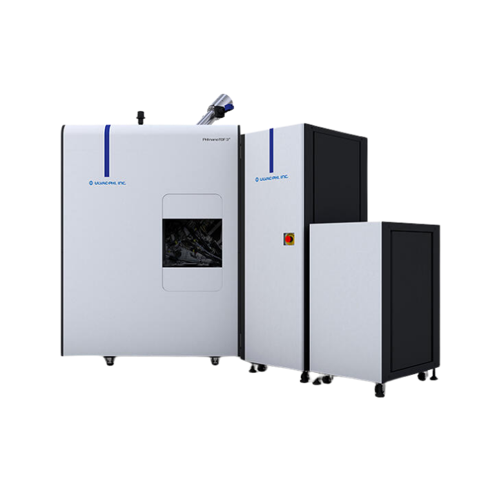
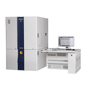
ULVAC PHI’s Latest Generation of TOF-SIMS, having a Modern Ergonomic Package, Smaller Footprint, and Advanced Features
KEY TECHNOLOGY
- High-precision analysis with TRIFT analyzer
- Continuous unattended measurement of insulating materials
- Unique ion beam technology
- Molecular structure analysis based on Parallel Imaging MS/MS
- A wide selections of options
Triple Focusing Electrostatic Analyzer
for Complex Sample Geometries
TRIFT Analyzer for a Wide Range of Sample Geometries,
Wide Bandpass Energy, and Wide Acquisition Angle
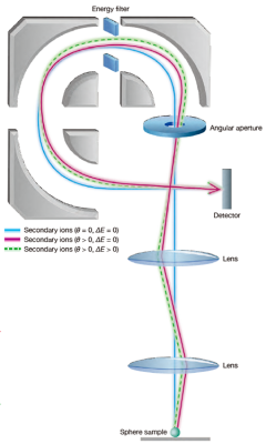
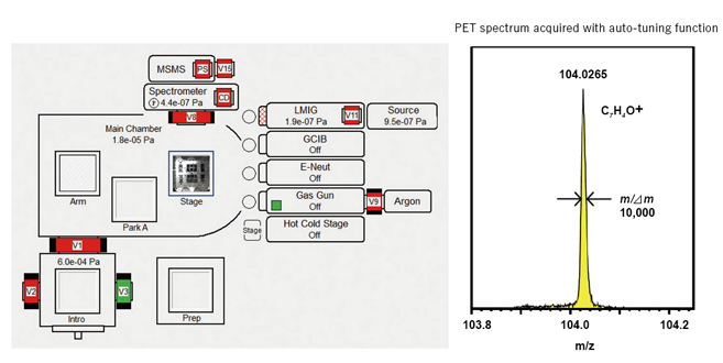
In exactly the same mass will have different flight times in the analyzer. This is particularly noticeable for samples with height differences or uneven surfaces.
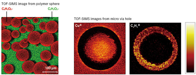
The Triple Ion Focusing Time-of-flight (TRIFT) spectrometer is able to simultaneously compensate for differences in flight time caused by differences in energy and emission angle. This is a key feature of the TRIFT spectrometer, which achieves high mass resolution and high detection sensitivity, as well as imaging with reduced shadows as demonstrated in the examples below.
Primary Ion Gun for High-Precision Analysis
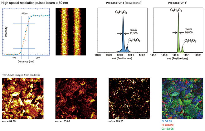
Advanced Ion Beam Technology Achieves High Spatial Resolution and High Mass Resolution
PHI nanoTOF 3+ offers TOF-SIMS analysis with a high spatial resolution of < 500 nm in high mass resolution mode and < 50 nm in high spatial resolution mode. The combination of a high brightness ion source, a high precision pulse mechanism and a high resolution spectrometer ensures low noise, high sensitivity and high resolution measurements. In both modes, measurements are completed within a few minutes.
The first-ever automated unattended TOF-SIMS analysis of multiple insulating samples
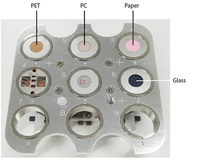 With the newly developed auto sample bias adjustment feature, it is now possible to perform unattended TOF-SIMS measurements on samples including insulating samples. The process is thoroughly simplified; 1) taking an intro photo, 2) selecting the analysis points on the intro photo, and 3) pressing the start button. In the past, skilled operators had to be dedicated to the instrument for analysis, but now the high quality data can be obtained regardless of operator skill.
Automated Sample Transport System and Parking Position as Standard
The instrument is equipped with an automatic sample transfer system that has been proven in more than 300 XPS Q-Series units. Sample sizes of up to 100 mm × 100 mm are possible, and the analysis chamber has a built-in parking position as standard. The system allows continuous automated unattended analysis of large numbers of samples.
Unique Ion Beam Technology
New Pulsed Argon Ion Gun for Complete Turnkey Charge Neutralization
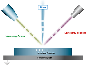
The pulsed low-energy electrons and argon ions can easily neutralize surface charge for both positive and negative ion polarities regardless of the type and shape of the insulating sample.
* For Ar ion gun option is selected.
FIB Fabrication Followed by Cross-section Imaging within a Single LMIG
FIB Function with Standard LMIG
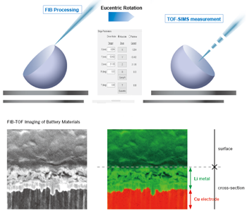
FIB processing function has newly been added to LMIG for primary ion source. This makes it possible to perform from FIB processing to cross-sectional TOFSIMS imaging with a single ion gun. Stage rotation is involved from processing to observation, but the Eucentric function allows the stage to return to the same field of view after rotation, easy identifying the FIB position.
To achieve 3D tomography, the dedicated Ga-FIB option is recommended. The Ga-FIB may be further optioned to operate as a second analysis beam.
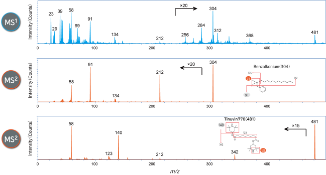
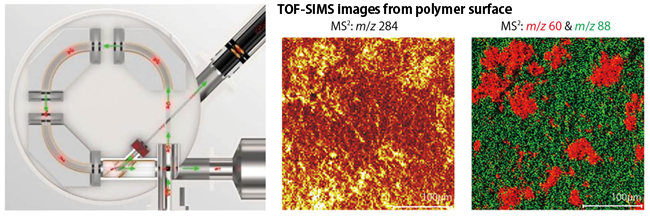
Molecular Structure Analysis based on Parallel Imaging MS/MS (Option)
Simultaneous Acquisition of MS1 and MS2 Data
By combining a tandem mass spectrometer (MS2) with a conventional TOF-SIMS analyzer (MS1), MS1 and MS2 data can be acquired simultaneously in the same measurement field with high sensitivity and speed.
The MS1 spectrum can be complex due to the large number of mass peaks generated by all components and fragments. Conversely, the MS2 spectrum, which is extracted and segmented by the precursor selector, has a much simpler spectral pattern. This provides information about the molecular structure, such as terminal groups, linear chains, or double bonds, and enables specific molecular structure imaging.
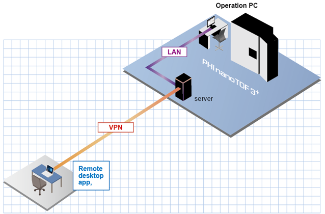
Reliable Remote Access for Measurements and Diagnostics, Even Away from the Instrument
Remote Access Function Allows the Instrument to be Controlled Remotely
The PHI nanoTOF 3+ allows you to access the instrument via your company’s local area network or the internet. Once the sample holder is mounted in the intro chamber, functions such as transferring the sample into the analysis chamber, sample holder exchange with the parking position, setting of the measurement conditions (including all options), and data acquisition can all be performed remotely. Diagnostics of the instrument hardware and electronics can also be accessed remotely.
* For more information on remote diagnostics, please contact our Customer Service Department.
Optional Accessories
- Parallel Imaging MS/MS
- Ar Gas Cluster Ion Beam Gun (GCIB)
- C60 Ion Gun
- Cs Ion Gun
- Ar/ O2 Gas Gun
- Hot/Cold Sample Stage Module
- High Temperature Sample Stage Module
- Transfer Vessel
- Oxygen Flood Module
- Focused Ion Beam (FIB) Gun
- FIB Software
- Sample Preparation Chambers
- Intro Chamber Glove Box
- Off-line Data Reduction Software
- Static SIMS Library


")
")


")
")
