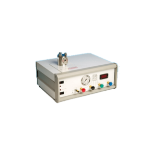
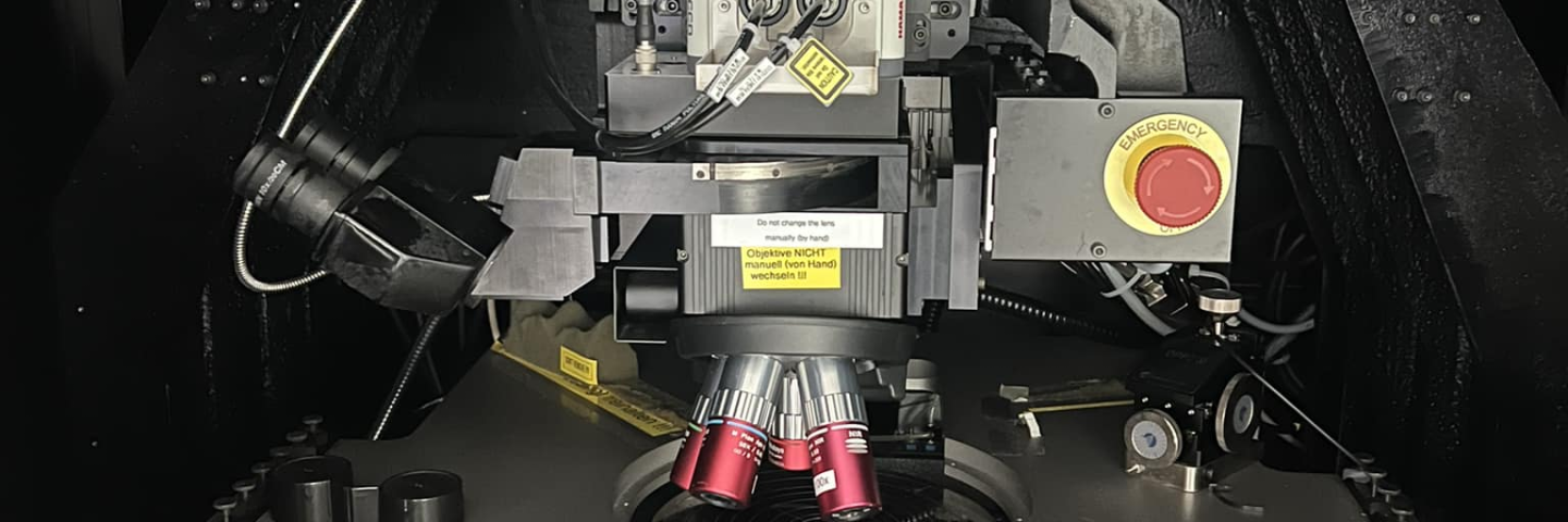
The AFM100 Series is Hitachi’s next generation probe microscopy platform. The AFM100 Plus and AFM100 systems that make up this series have been designed to expand the capabilities and performance of atomic force microscopy, while providing an easy-to-use platform suitable for users of all experience levels.
Experience the finest reliability and innovation with the AFM100 Series.

Hitachi Atomic Force Microscope AFM100 Multifunctional Probe Microscopy Platform

Pre-mounted cantilevers make replacement EASY(option)
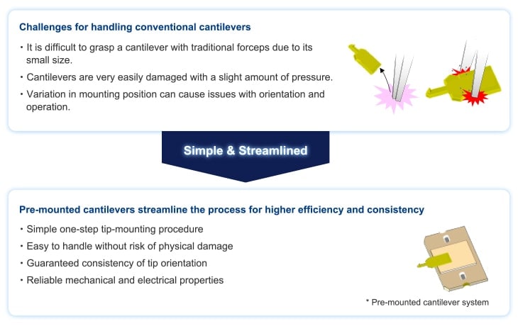
Pre-mounted cantilevers make replacement EASY(option)

Automated measurement & analysis with one-click autopilot function
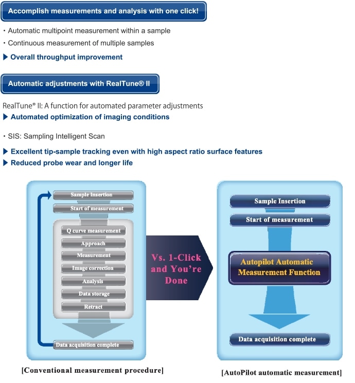
Automated measurement & analysis with one-click autopilot function

Correlative SEM-EDS Analysis with our AFM Marking Function

Analyze the same region of interest (ROI) with SEM, EDS, and AFM: More Information = Better Results!

  • Automated AFM Marking Features with Navigation Software.
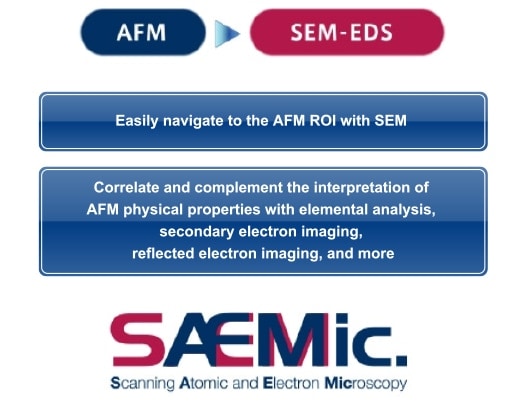
・Automated AFM Marking Features with Navigation Software.
※SÆMic. is a generic term for SEM-AFM correlative analysis recommended by Hitachi High-Tech.

[Evaluating AFM-KFM-SEM-EDS of Aluminum Alloy before and after Corrosion]

[Evaluating AFM-KFM-SEM-EDS of Aluminum Alloy before and after Corrosion]

Specifications

 AFM100 PlusAFM100
Detection System/Light SourceOptical lever/SLD (Super luminescent diode)
Lever holderPremount holder*, multi-holder*
Basic SpecificationsRMS noise level: ≦0.03 nm, in-plane drift: ≦0.03 nm/sec
Sample sizeMax. 35 mmφ, thickness 10 mm, (max. 50 mm sq., thickness 20 mm)*
Scanner (Scan range)*(XY:20 μm/Z:1.5 μm, XY:100 μm/Z:15 μm, XY:150 μm/Z:5 μm)*(Included with a 5-year warranty)
Light microscopeMicroscope with zoom function (Field of view XY:1.8 x 1.38 to 0.26 x 0.2 mm)*
Simple optical microscope (Field of view XY:1.6 x 1.2 mm)*
Simple optical microscope
(field of view XY:1.6 × 1.2 mm)
Basic functionsAFM, DFM, PM, FFM, SIS-shapes/properties, Q-value controlAFM, DFM, PM, FFM, SIS-shapes
Vibration isolation and noise isolation mechanismPassive vibration isolation air table and sound-proof coverStandard tabletop
Sample transfer mechanismManual Stage XY:±2.5 mm, Impact Stage Set (Conductive Type)*
Measurement environmentAtmosphere, in liquid*, heated* (room temperature to 250 °C), heated in liquid* (room temperature to 60 °C)
Other functionsSelf-check function, software download service, AFM marking*
Power Supply SpecificationsAC 100 V ± 10 V, 15 A, 1 line, D inoculated grounded receptacle

The asterisk (*) in the table indicates feature is optional.

For detailed specifications, please refer to the product specification sheet.
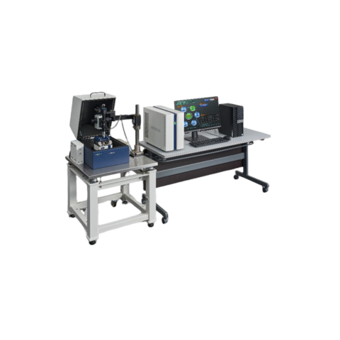
Hitachi Atomic Force Microscope AFM100 Multifunctional Probe Microscopy Platform

For more information, contact us. See more on Hitachi’s website

Features

Pre-mounted cantilevers make replacement EASY(option)

Pre-mounted cantilevers make replacement EASY(option)

Automated measurement & analysis with one-click autopilot function

Automated measurement & analysis with one-click autopilot function

Correlative SEM-EDS Analysis with our AFM Marking Function

Analyze the same region of interest (ROI) with SEM, EDS, and AFM: More Information = Better Results!

  • Automated AFM Marking Features with Navigation Software.
・Automated AFM Marking Features with Navigation Software.
※SÆMic. is a generic term for SEM-AFM correlative analysis recommended by Hitachi High-Tech.

[Evaluating AFM-KFM-SEM-EDS of Aluminum Alloy before and after Corrosion]

[Evaluating AFM-KFM-SEM-EDS of Aluminum Alloy before and after Corrosion]

Specifications

AFM100 Plus/AFM100 System Specifications
AFM100 Plus AFM100
Detection System/Light Source Optical lever/SLD (Super luminescent diode)
Lever holder Premount holder*, multi-holder*
Basic Specifications RMS noise level: ≦0.03 nm, in-plane drift: ≦0.03 nm/sec
Sample size Max. 35 mmφ, thickness 10 mm, (max. 50 mm sq., thickness 20 mm)*
Scanner (Scan range)* (XY:20 μm/Z:1.5 μm, XY:100 μm/Z:15 μm, XY:150 μm/Z:5 μm)*(Included with a 5-year warranty)
Light microscope Microscope with zoom function (Field of view XY:1.8 x 1.38 to 0.26 x 0.2 mm)*
Simple optical microscope (Field of view XY:1.6 x 1.2 mm)*
Simple optical microscope
(field of view XY:1.6 × 1.2 mm)
Basic functions AFM, DFM, PM, FFM, SIS-shapes/properties, Q-value control AFM, DFM, PM, FFM, SIS-shapes
Vibration isolation and noise isolation mechanism Passive vibration isolation air table and sound-proof cover Standard tabletop
Sample transfer mechanism Manual Stage XY:±2.5 mm, Impact Stage Set (Conductive Type)*
Measurement environment Atmosphere, in liquid*, heated* (room temperature to 250 °C), heated in liquid* (room temperature to 60 °C)
Other functions Self-check function, software download service, AFM marking*
Power Supply Specifications AC 100 V ± 10 V, 15 A, 1 line, D inoculated grounded receptacle

The asterisk (*) in the table indicates feature is optional.

For detailed specifications, please refer to the product specification sheet.

Related Products

The K850 combines versatility and ease of operation. Built-in thermo-electric heating and adiabatic cooling allow precise temperature control.
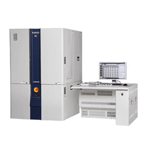
Hitachi High-Tech’s scanning electron microscopes SU3800/SU3900 deliver both operability and expandability. The operator can automate many operations and efficiently utilize their high performance.
ASAP-1® has become the standard preparation equipment that engineers involved in disciplines such as failure analysis, yield enhancement and competitive analysis.
Seiwa Wafer review system visually inspects the defect location detected from AOI systems. This review system is able to capture the visual data and add it to previous inspection results.
ULTRAPOL Basic lapping and polishing machine offers the build-quality required for high precision manual polishing of materials for production, research and NAND flash chip-off in digital forensics
The IM4000Plus Ion Milling System utilizes a broad, low-energy Ar+ ion beam milling method to produce wider, undistorted cross-section milling or flat milling.
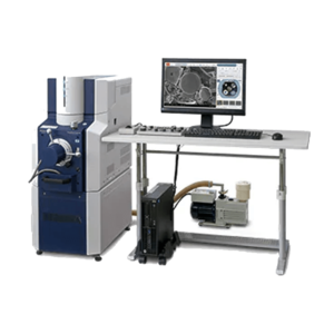
The Cold Field Emission source is ideal for high-resolution imaging with a small source size and energy spread. Innovative CFE Gun technology contributes the ultimate FE-SEM with superior beam bright
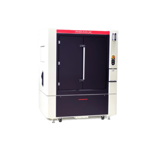
PHI’s Latest Generation of TOF-SIMS, having a Modern Ergonomic Package, Smaller Footprint, and Advanced Features
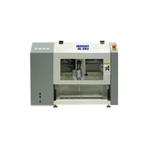
The IS-202 Scanning Acoustic Microscope combines highest resolution with a very compact mechanical set-up.
The only scanning Auger nanoprobe in the world that guarantees a field emission electron source whose spatial resolution is 8 nm or less.

How can we help?

You may contact our specialists by accomplishing form below.

failure analysis, material characterization, and metrology equipment

Subscribe to newsletter

Sign up for our newsletter to get updates on promos, seminars, events, products, application notes and more.

Inquire for this Product

AFM100
Multifunctional Probe Atomic Force Microscope
AFM100
Multifunctional Probe Atomic Force Microscope